Difference between revisions of "Whirlybird"
m (→M.2 (NGFF) Key E: U16:P0_5 corrected to Pin 54) |
m (Image with test cases) |
||
| (16 intermediate revisions by the same user not shown) | |||
| Line 11: | Line 11: | ||
Also used for [[Instant_Omni_Pro_18_Toaster_Oven_and_Air_Fryer|Singing "QSV" Toaster]] | Also used for [[Instant_Omni_Pro_18_Toaster_Oven_and_Air_Fryer|Singing "QSV" Toaster]] | ||
| + | |||
| + | Customized peripherals [[Whirlybird/IMU|IMU]] and [[Whirlybird/RS41|RS41]] | ||
| + | |||
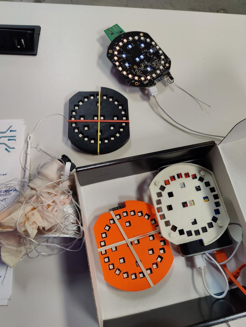
| + | [[File:Whirlybird 3D Printed Enclosure Tests.jpeg|800px]] | ||
= Components = | = Components = | ||
| + | |||
| + | == TPS54202DDCR Buck Converter (3v3) == | ||
| + | |||
| + | * Voltage In: 4.5-28 (12-28v typical) | ||
| + | * Voltage Out: Variable (5v typical) | ||
| + | * 2 Amp continuous, ~3 Amp current limit | ||
| + | * Over 90% Efficency 12v to 5v buck | ||
| + | * Package: SOT-6, Marking: "4202" | ||
| + | * [https://www.lcsc.com/datasheet/lcsc_datasheet_2410010331_Texas-Instruments-TPS54202DDCR_C191884.pdf Data Sheet] | ||
| + | |||
| + | Voltage In is provided from the first 4 pins of <code>J1</code> and this component is placed at <code>U9</code> with output voltage set point resistors <code>R25/R26</code> with values 100K and 22.1K respectively. Given the equation <code>(100/22.1 + 1) * 0.596 = 3.29</code>, the voltage output provided thru inductor <code>L2</code> in this configuration is set for 3.3 volts and provides the power to the ESP32 and related components. The 3v3 rail is also accessible at [TP](8) and voltage feedback at (TP13). | ||
| + | |||
| + | == LMR51440SDRRR Buck Converter (5v) == | ||
| + | * Voltage In: 4-36 | ||
| + | * Voltage Out: 0.8-28 | ||
| + | * Max Current: 4 Amp | ||
| + | * Package: 12 Pin WSON 0.8mm Height | ||
| + | * [https://www.lcsc.com/datasheet/lcsc_datasheet_2309221225_Texas-Instruments-LMR51450FNDRRR_C5782413.pdf Datasheet] | ||
| + | |||
| + | The component is placed at <code>U7</code> and there is a bodge jumping the voltage set point pin via <code>R19/R20</code> with a 1K resistor to correct for an in initial routing error of <code>R21/R18</code> ~18K and 100K respectively. This all results in a designed output voltage of 5 volts thru inductor <code>L1</code> and accessible at [TP](3) along with the voltage feedback at (TP10). | ||
== M.2 (NGFF) Key E == | == M.2 (NGFF) Key E == | ||
| Line 34: | Line 58: | ||
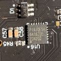
== PI4IOE5V6416 I2C GPIO Expander == | == PI4IOE5V6416 I2C GPIO Expander == | ||
*I2C Address: 0x20 (32) | *I2C Address: 0x20 (32) | ||
| − | *Part Number: | + | *Part Number: [https://www.diodes.com/datasheet/download/PI4IOE5V6416.pdf PI4IOE5V6416ZDEX] (TQFN) |
*Size: 4mm x 4mm | *Size: 4mm x 4mm | ||
*Pins: 24 | *Pins: 24 | ||
| Line 40: | Line 64: | ||
{| class="wikitable" | {| class="wikitable" | ||
|- | |- | ||
| − | ! Pin # !! Name !! Description | + | ! Pin # !! Name !! Description|Function |
|- | |- | ||
| − | | 1 || P0_0 || | + | | 1 || P0_0 || I/O M3 via R51 |
|- | |- | ||
| − | | 2 || P0_1 || | + | | 2 || P0_1 || I/O U6 & U8 Pin 3 (TP12,TP70) |
|- | |- | ||
| − | | 3 || P0_2 || | + | | 3 || P0_2 || I/O U56 |
|- | |- | ||
| − | | 4 || P0_3 || | + | | 4 || P0_3 || I/O M5 Pin 67 |
|- | |- | ||
| − | | 5 || P0_4 || | + | | 5 || P0_4 || GND M5 Pin 54 |
|- | |- | ||
| − | | 6 || P0_5 || | + | | 6 || P0_5 || U15 Pin 4 via R44 (TP67) |
|- | |- | ||
| − | | 7 || P0_6 || | + | | 7 || P0_6 || P3 Pin 6 (TP68) |
|- | |- | ||
| − | | 8 || P0_7 || | + | | 8 || P0_7 || (TP62) |
|- | |- | ||
| 9 || Vss || Ground | | 9 || Vss || Ground | ||
|- | |- | ||
| − | | 10 || P1_0 || | + | | 10 || P1_0 || U54 Pin 4 via R80 (TP73), R34 O Ohm GPIO 16 & U10 Pin 4 |
|- | |- | ||
| − | | 11 || P1_1 || | + | | 11 || P1_1 || J8 Pin 10 & R74 to GND (TP74) |
|- | |- | ||
| − | | 12 || P1_2 || | + | | 12 || P1_2 || U10 Pin 6 (TP75) |
|- | |- | ||
| − | | 13 || P1_3 || | + | | 13 || P1_3 || Select Input U11, HIGH for MicroSD SPI |
|- | |- | ||
| − | | 14 || P1_4 || | + | | 14 || P1_4 || U18 Pin 17 via R48 0 Ohm (TP77) |
|- | |- | ||
| − | | 15 || P1_5 || | + | | 15 || P1_5 || U17 Pin 1 (TOUT) & J9 & Pull-up via R7 |
|- | |- | ||
| − | | 16 || P1_6 || | + | | 16 || P1_6 || U1 Pin 4 (TP2,TP81) |
|- | |- | ||
| − | | 17 || P1_7 || | + | | 17 || P1_7 || J9 (TP80) |
|- | |- | ||
| 18 || ADDR || Address input, to Vdd or ground | | 18 || ADDR || Address input, to Vdd or ground | ||
| Line 84: | Line 108: | ||
| 21 || Vdd(P) || Power for Port P | | 21 || Vdd(P) || Power for Port P | ||
|- | |- | ||
| − | | 22 || INT || Interrupt output, connect to Vdd via pull-up resistor | + | | 22 || INT || ESP32 GPIO8. Interrupt output, connect to Vdd via pull-up resistor |
|- | |- | ||
| 23 || Vdd(I2C) || Power from I2C-bus, provides voltage-level translation | | 23 || Vdd(I2C) || Power from I2C-bus, provides voltage-level translation | ||
|- | |- | ||
| − | | 24 || RESET || Active LOW reset | + | | 24 || RESET || Active LOW reset (TP78), to Vdd via pull-up R45 10k |
|} | |} | ||
| Line 94: | Line 118: | ||
=== RGBW 5050 === | === RGBW 5050 === | ||
| + | * Inner Chain | ||
| + | ** U46,47,48,49,50,51,44,45 | ||
| + | ** Data in via R69 471 Ohm from U43 Pin 3 (TP118) | ||
| + | * Outer Chain | ||
| + | ** U24,23,22,21,20,19,30,29,28,27,26,25,36,35,34,33,32,31,42,41,40,39,38,37 | ||
| + | ** Data in via R68 471 Ohm from U43 Pin 2 (TP63) | ||
| + | * ~5 volt via R17, L1, U7, J1 and USB/Header | ||
* [https://cdn-shop.adafruit.com/product-files/2757/p2757_SK6812RGBW_REV01.pdf SK6812RGBW Datasheet (pdf)] | * [https://cdn-shop.adafruit.com/product-files/2757/p2757_SK6812RGBW_REV01.pdf SK6812RGBW Datasheet (pdf)] | ||
Note: May not be exact specification match for actual components used | Note: May not be exact specification match for actual components used | ||
| + | Connected to ESP32 via U43 (muxer?) | ||
=== Green 0603 === | === Green 0603 === | ||
| Line 203: | Line 235: | ||
[[User:-.-6eau|-.-6eau]] ([[User talk:-.-6eau|talk]]) 00:05, 4 October 2024 (UTC) | [[User:-.-6eau|-.-6eau]] ([[User talk:-.-6eau|talk]]) 00:05, 4 October 2024 (UTC) | ||
| + | |||
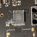
| + | === PI5L200 MUX === | ||
| + | |||
| + | U11 connected to GPIO 6, 7 & 15 SPI. Normally open logic path to MicroSD J5. | ||
| + | |||
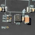
| + | Default connection is routed to M2 via U15, ''"scatch and sniff"'' for the routing RE win! | ||
| + | |||
| + | # Select Input U16 P1_3 grounded via 155K | ||
| + | # 1A0 Out to U15 Pin 1 | ||
| + | # 1A1 Out to MicroSD MISO | ||
| + | # YA In from GPIO 15 | ||
| + | # 1B0 Out to U15 Pin 16 | ||
| + | # 1B1 Out to MicroSD Clock | ||
| + | # YB In from GPIO 7 | ||
| + | # GND | ||
| + | # YC In from ? | ||
| + | # YC1 Out to ? | ||
| + | # YC0 Out to ? | ||
| + | # YD In from GPIO 6 | ||
| + | # YD1 Out to MicroSD MOSI | ||
| + | # YD0 Out to U15 Pin 14 | ||
| + | # Enable grounded (LOW enabled) | ||
| + | # Vcc | ||
| + | |||
| + | *https://www.digikey.com/en/products/detail/diodes-incorporated/PI5L200LE/1142607 | ||
| + | *https://mm.digikey.com/Volume0/opasdata/d220001/medias/docus/2380/PI5L200.pdf | ||
| + | |||
| + | == LCD == | ||
| + | *40 Pin Flat Flex connector at J8, backlight 18 volt boost from U54 enabled by GPIO Expand P1_0 or ESP32 GPIO 16. | ||
| + | *A number of pins are mux'd thru U18 and shared with camera. | ||
| + | *Looks to be RGB 8-bit per channel compatible, wired for RGB565 mode. | ||
| + | *Plausible match to: | ||
| + | **[https://cdn-shop.adafruit.com/product-files/2353/Datasheet.pdf 7" TFT 800x480 Datasheet] | ||
| + | **[https://cdn-shop.adafruit.com/product-files/1680/Datasheet.pdf 5" TFT 800x480 Datasheet] | ||
| + | |||
| + | == Camera == | ||
| + | *24 Pin Flat Flex connector at J10, lighting LEDs driven by U55. | ||
| + | *Signaling is mux'd with LCD thru U18 | ||
| + | *Plausible match to ESP32-CAM OV2640 | ||
== ESP32-S3-WROOM2 == | == ESP32-S3-WROOM2 == | ||
| Line 470: | Line 541: | ||
</pre> | </pre> | ||
| − | + | === Gallery === | |
| − | == | + | <gallery> |
| − | + | RGBW ESP32-S3 wiring RED-GREEN.png | |
| − | + | U18 SD642AO.jpg | |
| − | + | U11 PI5L200LE.jpg | |
| − | + | U16 PI4IOE5V9535.jpg | |
| + | D6 USBLC6-2SC6.jpg | ||
| + | U15 AKK 7YW.jpg | ||
| + | U55 PCA9632TK.jpg | ||
| + | Whirlybird Scratch and Sniff via Probing.jpeg | ||
| + | Whirlybird Camera Flat Flex.jpeg | ||
| + | </gallery> | ||
Latest revision as of 23:00, 12 October 2024
[EXPERIMENTAL] Direction Finding (DF)
This is an exercise that started with up-cycling some e-waste that contains 32 RGBW LEDs and an ESP32-S3-WROOM2. There is a myriad of other components presumably intended to interface with other control circuits.
The primary objective here is not to reverse engineer its previously intended purpose, rather invent a new purpose. The objective is to utilize the outer ring of 24 blinkies as a 360 degree direction indicator. The ESP32 module, which appears to never have been flashed with functioning firmware, is erased and flashed with a current Octal SPI build of Micropython.
For the most part the components on the PCB are not directly connected to the ESP32. Rather there is a number of connectors they are wired to for an alternative "main" processor. This includes the addressable RGBWs that are some variant of SK6812RGBW. Additionally for some reason even though these are individually addressable in series of over a hundred, they are broken in to two independent chains of 24 spaced in an outer circular pattern and 8 more arranged inside that circle.
The board is likely designed as some sort of prototype of an evolution of a production product. It is unknown if it was intended to be a technical evaluation of various features, in ongoing development or a one off experiment. I have ended up with several dozen of these, there are many unknown and some number of issues. The majority of them have thus far had an issue with enabling "Boot Mode" and power on only to continually restart themselves.
Also used for Singing "QSV" Toaster
Customized peripherals IMU and RS41
Contents
Components
TPS54202DDCR Buck Converter (3v3)
- Voltage In: 4.5-28 (12-28v typical)
- Voltage Out: Variable (5v typical)
- 2 Amp continuous, ~3 Amp current limit
- Over 90% Efficency 12v to 5v buck
- Package: SOT-6, Marking: "4202"
- Data Sheet
Voltage In is provided from the first 4 pins of J1 and this component is placed at U9 with output voltage set point resistors R25/R26 with values 100K and 22.1K respectively. Given the equation (100/22.1 + 1) * 0.596 = 3.29, the voltage output provided thru inductor L2 in this configuration is set for 3.3 volts and provides the power to the ESP32 and related components. The 3v3 rail is also accessible at [TP](8) and voltage feedback at (TP13).
LMR51440SDRRR Buck Converter (5v)
- Voltage In: 4-36
- Voltage Out: 0.8-28
- Max Current: 4 Amp
- Package: 12 Pin WSON 0.8mm Height
- Datasheet
The component is placed at U7 and there is a bodge jumping the voltage set point pin via R19/R20 with a 1K resistor to correct for an in initial routing error of R21/R18 ~18K and 100K respectively. This all results in a designed output voltage of 5 volts thru inductor L1 and accessible at [TP](3) along with the voltage feedback at (TP10).
M.2 (NGFF) Key E
- Part #: MDT420E03001
- Amphenol Product Page
- Brochure
- PCIe M.2 Connectors, Storage and Server Connector, P=0.5mm, H=4.2mm, Key E,Gold Plating
WARNING Pin out is not compatible with typical specifications!
Top is odd, bottom is even
- Ground Pins: 3,5,11,18,33,39,45,51,57,71,73
- 3v3 Pins: 2 & 4
- D+/D- Pins: 7 & 9 (via D6) to J7
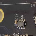
- Tx/Rx Pins: 62 & 64 (via R37/R35)
- U16:P0_5 Pin: 54 (TP72)
- U16:P0_4 Pin: 67 (via Q1) to ground
- TP85-92 Pins: 38,46,48,50,52,56,58,60
PI4IOE5V6416 I2C GPIO Expander
- I2C Address: 0x20 (32)
- Part Number: PI4IOE5V6416ZDEX (TQFN)
- Size: 4mm x 4mm
- Pins: 24
| Pin # | Name | Function |
|---|---|---|
| 1 | P0_0 | I/O M3 via R51 |
| 2 | P0_1 | I/O U6 & U8 Pin 3 (TP12,TP70) |
| 3 | P0_2 | I/O U56 |
| 4 | P0_3 | I/O M5 Pin 67 |
| 5 | P0_4 | GND M5 Pin 54 |
| 6 | P0_5 | U15 Pin 4 via R44 (TP67) |
| 7 | P0_6 | P3 Pin 6 (TP68) |
| 8 | P0_7 | (TP62) |
| 9 | Vss | Ground |
| 10 | P1_0 | U54 Pin 4 via R80 (TP73), R34 O Ohm GPIO 16 & U10 Pin 4 |
| 11 | P1_1 | J8 Pin 10 & R74 to GND (TP74) |
| 12 | P1_2 | U10 Pin 6 (TP75) |
| 13 | P1_3 | Select Input U11, HIGH for MicroSD SPI |
| 14 | P1_4 | U18 Pin 17 via R48 0 Ohm (TP77) |
| 15 | P1_5 | U17 Pin 1 (TOUT) & J9 & Pull-up via R7 |
| 16 | P1_6 | U1 Pin 4 (TP2,TP81) |
| 17 | P1_7 | J9 (TP80) |
| 18 | ADDR | Address input, to Vdd or ground |
| 19 | SCL | Clock to Vdd via pull-up resistor |
| 20 | SDA | Data to Vdd via pull-up resistor |
| 21 | Vdd(P) | Power for Port P |
| 22 | INT | ESP32 GPIO8. Interrupt output, connect to Vdd via pull-up resistor |
| 23 | Vdd(I2C) | Power from I2C-bus, provides voltage-level translation |
| 24 | RESET | Active LOW reset (TP78), to Vdd via pull-up R45 10k |
LEDs
RGBW 5050
- Inner Chain
- U46,47,48,49,50,51,44,45
- Data in via R69 471 Ohm from U43 Pin 3 (TP118)
- Outer Chain
- U24,23,22,21,20,19,30,29,28,27,26,25,36,35,34,33,32,31,42,41,40,39,38,37
- Data in via R68 471 Ohm from U43 Pin 2 (TP63)
- ~5 volt via R17, L1, U7, J1 and USB/Header
- SK6812RGBW Datasheet (pdf)
Note: May not be exact specification match for actual components used
Connected to ESP32 via U43 (muxer?)
Green 0603
- Part Number: LTST-C193TGKT-5A
- Digi-Key #: 160-1832-1-ND
- Description: LED GREEN CLEAR CHIP SMD
- Size: 0603, 1.6mm x 0.8mm x 0.45mm
- Wavelength: 528nm
These are used for testing and some have been populated at D8-D16. Depending on how many are used they are 0-3 in parallel connected to the PCA9632 driver. Do to the lack of current limiting resistor and the high supply voltage, they tolerated a good level of abuse working out the appropriate PWM control for less than the rated 20mA.
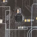
PCA9632 I2C driver
4-bit Fm+ I2C-bus low power LED driver
- I2C Address: 0x62 (98)
- Type: PCA9632TK
- Marking: 9632
- Package: HVSON8
- plastic thermal enhanced very thin small outline package
- no leads
- 8 terminals
- body 3 × 3 × 0.85 mm with 0.5 mm pitch
- Version: SOT908-1
This component is placed at U55 with LED0, LED1 & LED2 connected in groups of up to 3 LEDs in parallel providing a path to ground with the positive side of each LED going directly to >4 volts without a current limiting resistor. Using a PWM power value of 0xF0 or less seems to be quite reasonable and it is still quite visible with 0x01-0x05 as well, at least with the tested #Green 0603 singularly or in a parallel pair.
Note: Datasheet claims that LEDOUT register supports LEDs are on, off, individual dimming or individual dimming and group dimming/blink. The individual dimming and group control states were only exclusively selectable in testing with bits 10, 11 for individual vs group control respectively.
| Name | Pin | Type | Description |
|---|---|---|---|
| LED0 | 1 | Out | LED driver 0 |
| LED1 | 2 | Out | LED driver 1 |
| LED2 | 3 | Out | LED driver 2 |
| LED3 | 4 | Out | LED driver 3 |
| GND | 5 | - | Ground |
| SCL | 6 | In | I2C Clock |
| SDA | 7 | In/Out | I2C Data |
| VDD | 8 | + | Power Supply |
Minimal test code, demonstrates individual channel dimming and group blink. Green LEDs were added to D8, D11, & D12.
# PCA9632 I2C 4-Bit LED Driver by DEFAULT
from machine import Pin, SoftI2C, Timer
from time import sleep_ms
# I2C Address for LED Driver for D8-D16
ADDR = 0x62
# Register Addresses
MODE1 = 0x00   # 0x10=on,0x00=sleep
MODE2 = 0x01   # 0x00=dim,0x20=blink(group)
# 8-bit individual brightness
PWM0 = 0x02    # D11,D8,D14
PWM1 = 0x03    # D9,D10,D12
PWM2 = 0x04    # D16,D15,D13
PWM3 = 0x05    # not connected
# Group control
GRPPWM = 0x06  # 7-bit
GRPFREQ = 0x07 # 7-bit
# 0[1:0],1[3:2],2[5:4],3[7:6]
# 00=Off,01=On,10=PWMx,11=GRPPWM
LEDOUT = 0x08

# Whirlybird I2C (4+ devices connected)
i2c = SoftI2C(scl=4, sda=5, freq=100_000)

blinking = True

def write(reg,val):
 i2c.writeto_mem(ADDR, reg, bytearray([val]))

def dim():
 write(PWM0, 0x05)   # D8 & D11
 write(PWM1, 0x03)   # D12
 write(LEDOUT, 0x0A) # Enable PWM0 & PWM1
 write(MODE2, 0x00)

def blink():
 write(GRPPWM,0x0F)  # Group brightness
 write(GRPFREQ,0x0F) # Group blink rate
 write(LEDOUT, 0x0F) # Enable DMBLNK
 write(MODE2, 0x20)

def toggleMode(t):
 global blinking
 if blinking:
  dim()
 else:
  blink()
 blinking = not blinking

write(MODE1,0x00)    # Power on Driver
toggleMode(None)     # Start in Dimming
-.-6eau (talk) 00:05, 4 October 2024 (UTC)
PI5L200 MUX
U11 connected to GPIO 6, 7 & 15 SPI. Normally open logic path to MicroSD J5.
Default connection is routed to M2 via U15, "scatch and sniff" for the routing RE win!
- Select Input U16 P1_3 grounded via 155K
- 1A0 Out to U15 Pin 1
- 1A1 Out to MicroSD MISO
- YA In from GPIO 15
- 1B0 Out to U15 Pin 16
- 1B1 Out to MicroSD Clock
- YB In from GPIO 7
- GND
- YC In from ?
- YC1 Out to ?
- YC0 Out to ?
- YD In from GPIO 6
- YD1 Out to MicroSD MOSI
- YD0 Out to U15 Pin 14
- Enable grounded (LOW enabled)
- Vcc
- https://www.digikey.com/en/products/detail/diodes-incorporated/PI5L200LE/1142607
- https://mm.digikey.com/Volume0/opasdata/d220001/medias/docus/2380/PI5L200.pdf
LCD
- 40 Pin Flat Flex connector at J8, backlight 18 volt boost from U54 enabled by GPIO Expand P1_0 or ESP32 GPIO 16.
- A number of pins are mux'd thru U18 and shared with camera.
- Looks to be RGB 8-bit per channel compatible, wired for RGB565 mode.
- Plausible match to:
Camera
- 24 Pin Flat Flex connector at J10, lighting LEDs driven by U55.
- Signaling is mux'd with LCD thru U18
- Plausible match to ESP32-CAM OV2640
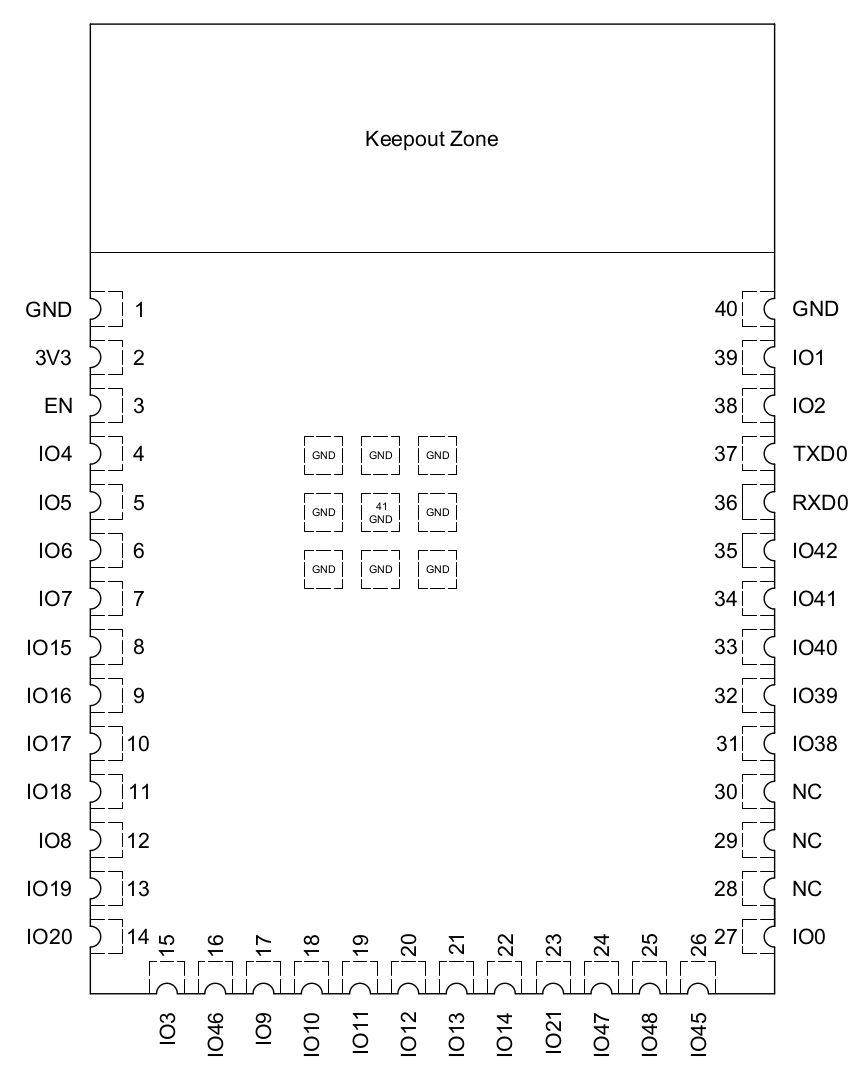
ESP32-S3-WROOM2
Pin Layout
Firmware
When connecting to a linux machine, the following can be seen via dmesg | tail.
new full-speed USB device number 99 using xhci_hcd
New USB device found, idVendor=303a, idProduct=1001, bcdDevice= 1.01
New USB device strings: Mfr=1, Product=2, SerialNumber=3
Product: USB JTAG/serial debug unit
Manufacturer: Espressif
SerialNumber: 68:B6:B3:##:##:##
cdc_acm 3-2:1.0: ttyACM0: USB ACM device
While the device enumerates with USB connected and has the capacity to facilitate serial communications, it is not really feasible with the constant reboot cycle. There are two slight variations of the board, the ones with a populated micro SD slot mostly have this issue, and the others do not. However connecting to the TXD0 pin to the Rx of a USB/Serial UART converter the following can be captured. Additionally holding the ESP32 in reset and monitoring the UART you can capture the following by briefly releasing the reset and then re-enabling reset, otherwise you will get a continuous flood of the same messages at 115200 baud.
ESP-ROM:esp32s3-20210327
Build:Mar 27 2021
rst:0x1 (POWERON),boot:0x8 (SPI_FAST_FLASH_BOOT)
invalid header: 0xa5ff005a
invalid header: 0xa5ff005a
invalid header: 0xa5ff005a
invalid header: 0xa5ff005a
Further experimentation is indicating it may be related to a fault in the thru-hole GPI0 as directly shorting GPIO0 (Pin 27) to ground can result in the following.
ESP-ROM:esp32s3-20210327
Build:Mar 27 2021
rst:0x1 (POWERON),boot:0x36 (SPI_DOWNLOAD_BOOT)
wait spi download
ESP-ROM:esp32s3-20210327
Build:Mar 27 2021
rst:0x15 (USB_UART_CHIP_RESET),boot:0x36 (SPI_DOWNLOAD_BOOT)
Saved PC:0x400507ae
wait spi download
Attempting to use esptool.py generates a Connecting... message and then the serial output generates and updated message.
ESP-ROM:esp32s3-20210327
Build:Mar 27 2021
rst:0x15 (USB_UART_CHIP_RESET),boot:0x36 (SPI_DOWNLOAD_BOOT)
Saved PC:0x400507ae
wait spi download
However this seems to hang the USB connection and nothing further happens until it times out.
Update: the results above have been the result of GPIO46 (Pin 16) floating. This is resolved by pulling it to ground along with GPIO0 to properly enable USB/UART0 for flashing. This can also be achieved using TP50 which also connects to GPI046.
Some of the boards do properly enter "Boot Mode" which is done by connecting GPIO0 to ground. This can easily be done by using a jumper wire from a through hole header that exposes both GPIO0 and ground and pressing a reset button immediately below it. Alternatively this can be achieved by using a wire pressed to the bottom right most module pin and the metal RF shield on top of the module while connecting USB to power on.
Successfully resetting with GPIO0 low and monitoring the Tx pin output, the device will send the following when properly configured and enabled to work with esptool.py.
Build:Mar 27 2021
rst:0x1 (POWERON),boot:0x0 (DOWNLOAD(USB/UART0))
waiting for download
For first time use with Micropython a complete erase of flash should first be performed with the following,
esptool.py -p /dev/ttyACM0 -b 115200 erase_flash
esptool.py v4.8.0
Serial port /dev/ttyACM0
Connecting...
Detecting chip type... ESP32-S3
Chip is ESP32-S3 (QFN56) (revision v0.1)
Features: WiFi, BLE, Embedded PSRAM 8MB (AP_1v8)
Crystal is 40MHz
MAC: 68:b6:b3:3c:f4:24
Uploading stub...
Running stub...
Stub running...
Erasing flash (this may take a while)...
Chip erase completed successfully in 70.8s
Hard resetting via RTS pin...
Note in this instance RTS is not connected, however the device remains in "Boot Mode" and the following action can be performed.
esptool.py -p /dev/ttyACM0 -b 1500000 write_flash -z 0 ESP32_GENERIC_S3-SPIRAM_OCT-20240920-v1.24.0-preview.335.gb08ddbba5.bin
esptool.py v4.8.0
Serial port /dev/ttyACM0
Connecting...
Detecting chip type... ESP32-S3
Chip is ESP32-S3 (QFN56) (revision v0.1)
Features: WiFi, BLE, Embedded PSRAM 8MB (AP_1v8)
Crystal is 40MHz
MAC: 68:b6:b3:3c:f4:24
Uploading stub...
Running stub...
Stub running...
Changing baud rate to 1500000
Changed.
Configuring flash size...
Flash will be erased from 0x00000000 to 0x00197fff...
Compressed 1668096 bytes to 1089606...
Wrote 1668096 bytes (1089606 compressed) at 0x00000000 in 18.7 seconds (effective 714.0 kbit/s)...
Hash of data verified.

Leaving...
Hard resetting via RTS pin...
Note that in this case without RTS the device must be manually power cycled or reset to load the new firmware. Now you should see a different enumeration via dmesg.
new full-speed USB device number 41 using xhci_hcd
New USB device found, idVendor=303a, idProduct=4001, bcdDevice= 1.00
New USB device strings: Mfr=1, Product=2, SerialNumber=3
Product: Espressif Device
Manufacturer: Espressif Systems
SerialNumber: 123456
cdc_acm 3-2:1.0: ttyACM0: USB ACM device
Monitoring TXD0 the following is received.
ESP-ROM:esp32s3-20210327
Build:Mar 27 2021
rst:0x1 (POWERON),boot:0x2a (SPI_FAST_FLASH_BOOT)
SPIWP:0xee
Octal Flash Mode Enabled
For OPI Flash, Use Default Flash Boot Mode
mode:SLOW_RD, clock div:1
load:0x3fce3820,len:0x105c
load:0x403c9700,len:0x4
load:0x403c9704,len:0xbd8
load:0x403cc700,len:0x2e34
entry 0x403c989c
MicroPython v1.24.0-preview.335.gb08ddbba5 on 2024-09-20; Generic ESP32S3 module with Octal-SPIRAM with ESP32S3
Type "help()" for more information.
>>>
You can also now use the USB interface, with something like screen /dev/ttyACM0 115200. If successful you should be greeted with blank output. Pressing Enter should generate a Micropython prompt >>> and pressing Ctrl+D generates the following.
MPY: soft reboot
MicroPython v1.24.0-preview.335.gb08ddbba5 on 2024-09-20; Generic ESP32S3 module with Octal-SPIRAM with ESP32S3
Type "help()" for more information.
>>>
There's various ways you can now access the device, including over WiFi once configured. I highly recommend rshell which provides the ability to copy and move files as well as directly write and debug code using REPL. If you don't pass any arguments it will automatically attempt to connect, if you have multiple devices you can also specify the connection parameters. Here the built in USB/Serial interface is connected via D+/D- pins.
rshell -p /dev/ttyACM0 -b 115200
Using buffer-size of 256
Connecting to /dev/ttyACM0 (buffer-size 256)...
Trying to connect to REPL  connected
Retrieving sysname ... esp32
Testing if ubinascii.unhexlify exists ... Y
Retrieving root directories ... /boot.py/ /main.py/
Setting time ... Sep 26, 2024 09:42:01
Evaluating board_name ... pyboard
Retrieving time epoch ... Jan 01, 2000
Welcome to rshell. Use Control-D (or the exit command) to exit rshell.
Once launched, any running code may be halted, entering repl will give an interactive Micropython prompt. Entering Ctrl+D will do a soft reset and any code configured to automatically start such as main.py will then run and you will see any output such as from print() in the terminal.
BOM
# Whirlybird "ECPB-00011-000 1/18/2024"


# Top RGBW Side
U10 "ZMYC" 6 pin
U13 "16248" 16 pin (2x8) no lead package
U15 "AKK 7YW +" 16 pin (4x4) no lead package
U43 "R5 0401 235" SOIC-8
# RGBW 5050 Inner
U46 0 center right
U47 1 center left
U48 2 far left
U49 3 lower left
U50 4 lower center
U51 5 lower right
U44 6 far right
U45 7 top center
# RGBW 5050 Outer
U24 0 top right of center
U23 1
U22 2
U21 3
U20 4
U19 5 3 O'clock furthest right middle
U30 6
U29 7
U28 8
U27 9
U26 10
U25 11 6 O'clock lowest center
U36 12
U35 13
U34 14
U33 15
U32 16
U31 17 9 O'clock furthest left middle
U42 18
U41 19
U40 20
U39 21
U38 22
U37 23 12 O'clock highest center
J3 Vcc Rx Tx GND RST 0
TP1
TP3
TP5
TP7
TP85-92 Top right to M5 pins
TP50 GPIO46 & U18
CAP_WIRE capacitive touch wire connection


# Bottom ESP32 Side
C18,19 "47 HFT S73" Electrolytic
D1 "TV7 J9" 6 lead
D2 "B5 J" (next to RST1)
D3 "S8 D0" J3 header power input
D4 "S8 D0" USB power input
D5 USB Connection ESD 6 pin (top/left)
D6 USB Connection ESD 6 pin (left side)
D7 "S8 D0" USB power input
J1 2x8 Connector
J4,J7 Micro USB Connector
J5 MicroSD slot
J8 "2272N50" 40-Pin Flat Flex Connector
J9 6 pin flat flex
L1 "5R6"
L2 "100 2229"
M5 "Amphenol E"
M3B 12-pin flat flex
P1 10 pin JTAG pads
R2,3,6,7 0 Ohm
R27 "01C" (next to RST1)
RST1 Tacticle momentary switch
U1 "2NMT" 6 lead
U2 "2NMT" 6 lead
U3 "2NMT" 6 lead
U4 "2NMT" 6 lead
U6 "WXM" 5 lead 2x3
U7 "L5144S TI 328 AGCS"
U8 "LN8B" 5 lead 2x3
U9 "4202" 6 lead
U16 "PI410E5V 6416ZDE 2341GG"
U17 "22-Biw" Capacitice Touch
U52 "JE3h4" 3 lead
U53 "F9 NZ" 8 pin lead
U54 "GEC"
U55 PCA9632 "9632 78 05 D335" 2x4 no lead package
U56 "1C7H 358 AFF 5" 6 pin no lead package
