Roland DIF-AT: Difference between revisions
→Cutter -: details |
|||
| (66 intermediate revisions by the same user not shown) | |||
| Line 1: | Line 1: | ||
PCB photos, Pinouts, Pin header, Device operation, Connections between subsystems. Notes on firmware structure, Machine language monitor program, DFU, firmware extraction, firmware update script (python)[[File:DIFAT 24.jpg|thumb|Roland publicity image |alt=]] | |||
PCB photos, Pinouts, Pin header, Device operation, Connections between subsystems. Notes on firmware structure, Machine language monitor program, DFU, firmware extraction, firmware update script (python) | |||
[[File:DIFAT 24.jpg|thumb|Roland publicity image |alt=]] | |||
===Brief outline -=== | ===Brief outline -=== | ||
I bought this device to repair. They are rare, and interesting. It would not respond any longer or be recognised by host hardware. | I bought this device to repair. They are rare, and interesting. It would not respond any longer or be recognised by host hardware. | ||
(it runs in conjunction with host digital mixer / host music production device, translating digital audio formats in real time) | (it runs in conjunction with host digital mixer / host music production device, translating digital audio formats in real time) | ||
[https://www.roland.com/br/products/dif-at24/ Roland's page on the DIF-AT] | |||
I damaged a lot of traces on the device and gave up on it. However, I learned how to micro-solder and became inspired to continue the repair with reverse engineering techniques. This is my first reverse engineering project, though I have worked on modding and repairing before. | I damaged a lot of traces on the device and gave up on it. However, I learned how to micro-solder and became inspired to continue the repair with reverse engineering techniques. This is my first reverse engineering project, though I have worked on modding and repairing before. | ||
| Line 17: | Line 13: | ||
===Goals-=== | ===Goals-=== | ||
#De-solder NOR Flash and read firmware. | #De-solder NOR Flash and read firmware. | ||
#Determine potential corruption of firmware. | #Determine potential corruption of firmware. | ||
#Re-flash firmware onto new NOR flash (if good). | #Re-flash firmware onto new NOR flash (if good). | ||
#Determine operation / | #Determine operation / corruption of Xilinx CPLD/Alesis IC - read contents. | ||
#Analyse firmware for anything interesting. | #Analyse firmware for anything interesting. | ||
#Determine and examine / analyse hardware architecture. | #Determine and examine / analyse hardware architecture. | ||
| Line 45: | Line 40: | ||
==Device Overview== | ==Device Overview== | ||
This is a complex device with a 16 bit CPU, Xilinx 95xx CPLD, Custom Alesis chip (Gate array, PAL, GAL, OTP CPLD?) SRAM, NOR flash 512kb, logic and switching for bus arbitration. BREQ Bus request is a very involved circuit. Also CE# Chip Enable NOR Flash is connected through a complicated muxing circuit. The Alesis custom IC handles the WE# Write Enable to the NOR Flash. | This is a complex device with a 16 bit CPU, Xilinx 95xx CPLD, Custom Alesis chip (ASIC, Gate array, PAL, GAL, OTP CPLD?) SRAM, NOR flash 512kb, logic and switching for bus arbitration. BREQ Bus request is a very involved circuit. Also CE# Chip Enable NOR Flash is connected through a complicated muxing circuit. The Alesis custom IC handles the WE# Write Enable to the NOR Flash, and also seems BREQ master. | ||
No info could be found on the Alesis chip, searching for the numerous IC markings revealed nothing. | No info could be found on the Alesis chip, searching for the numerous IC markings revealed nothing. After more research, it seems likely it is an ASIC, as the functions it performs are advanced. | ||
The Device is quite old school. This was built for the early generation of ADAT/TDIF machines, still using physical tape. Thankfully a tape machine is not necessary for operation. The sync requirements of locking digital audio using analogue tape definitely adds complexity to this system. | The Device is quite old school. This was built for the early generation of ADAT/TDIF machines, still using physical tape. Thankfully a tape machine is not necessary for operation. The sync requirements of locking digital audio using analogue tape definitely adds complexity to this system. | ||
Device has 2 buttons on the PCB: 1 - RESET, reset circuit | Device has 2 buttons on the PCB: '''Switch 1''' - RESET, reset circuit (dedicated IC) '''Switch''' '''2''' - Launch monitor diagnostic mode. | ||
A 50 pin header provides easy access to most address lines and relevant (to operation) CPU/RAM/Flash lines. This will be convenient to run a logic capture during boot and operation later. I beeped out the 50 pin connector - Many pins have multiple connections. Happily; the vias were not tented - this was a long endeavour even with continuity through the vias : ) Below, the findings and some general notes: | |||
<gallery> | |||
File:DIFat 50 pin header1 .png|alt=dif at pin header pins 1 - 16|'''Header pins 1 - 16''' | File:DIFat 50 pin header1 .png|alt=dif at pin header pins 1 - 16|'''Header pins 1 - 16''' | ||
File:DIFat 50 pin header2.png|alt=header pins 16 - 24|'''Header pins 16 - 24''' | File:DIFat 50 pin header2.png|alt=header pins 16 - 24|'''Header pins 16 - 24''' | ||
| Line 63: | Line 60: | ||
==JTAG/Programming/CPLD== | ==JTAG/Programming/CPLD== | ||
The device has two levels of firmware: NOR Flash and CPLD bitstream. The Xilinx is an older model XC95144 which is programmed over JTAG. However | The device has two levels of firmware: NOR Flash and CPLD bitstream. The Xilinx is an older model XC95144 which is programmed over JTAG. However (as I understand it) due to the architecture: bitstream cannot be read out over JTAG (even if unlocked) It has to use vendor specific tools (Platform Cable USB) in order to recover the bitstream. | ||
JTAG pads are exposed on the PCB as seen in the image above. I could connect to these to read the CPLD. Pretty soon they were pulled off the board, and I had to solder a pin to the leg temporarily to continue reading data. (before I discovered tiny IC clips!) | JTAG pads are exposed on the PCB as seen in the image above. I could connect to these to read the CPLD. Pretty soon they were pulled off the board, and I had to solder a pin to the leg temporarily to continue reading data. (before I discovered tiny IC clips!) | ||
[Only one device is visible in the JTAG chain, the Xilinx. The CPU, H8300H (Hitachi/Renesas) is not equipped with JTAG at all. Low level CPU operation is done through a bootloader mode] | [Only one device is visible in the JTAG chain, the Xilinx. The CPU, [https://www.alldatasheet.com/datasheet-pdf/download/249501/RENESAS/H8SLASH300H.html H8300H] (Hitachi/Renesas) is not equipped with JTAG at all. Low level CPU operation is done through a bootloader mode] Interesting and lovely late 1990s marketing publication [https://www.ele.uva.es/~jesman/BigSeti/ftp/Microcontroladores/Hitachi/H8-300H/h8_16bit.pdf here] | ||
I connected to the [https://www.datasheet.live/pdfviewer?url=https%3A%2F%2Fwww.datasheet.live%2Fdatasheet%2Fxilinxsemi%2FXC95144XL-7TQ100C0962.pdf Xilinx XC95144] using [https://github.com/Aodrulez/blueTag/tree/main Bluetag], [https://openocd.org/ OpenOCD] and [https://github.com/MPLew-is/xc3sprog XC3SPROG] (open source Xilinx CLI) and was eventually able to read back ID codes and find IR Len etc. I was happy it was responding. It was fun, confusing and difficult to set up all these tools. I set most of them up on a Raspberry Pi as dedicated hacking server so I can connect remotely to the hot mess setup with my laptop, somewhere more comfortable : ) | |||
It seems strange to me that, this is a 100 pin CPLD, and only 4 inputs and 4 outputs are used! (solely RBUS data, 8 channels L/R in/out). Counter output from H8300H goes to clock pin of the Xilinx, through an inverter. | |||
<gallery> | <gallery> | ||
File:XC3SPROG id read.png|alt=XC3SPROG id read|'''XC3SPROG id read''' | File:XC3SPROG id read.png|alt=XC3SPROG id read|'''XC3SPROG id read''' | ||
| Line 80: | Line 78: | ||
===BSDL Scan -=== | ===BSDL Scan -=== | ||
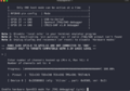
After initial ID code read, I used a [https://github.com/viveris/jtag-boundary-scanner BSDL GUI] to determine whether the CPLD was actually passing data throughput. Whilst easy to use when running, this tool took a while to set up (I mistakenly compiled it from source in Windows 7 32 bit - somehow missing the fact there there was a package release) After downloading the BSDL language file from Xilinx and setting up the tool with info from the Xilinx datasheet (super confusing naming convention, cells vs physical pins). Scanner could only run with this set up in Extest mode (OS not present nor running) toggling the input pins at a user defined frequency - means the corresponding output logic pulses accordingly. | [[File:VIVERIS BOUNDARY SCANNER.png|thumb|Viveris JTAG Boundary Scanner]]After initial ID code read, I used a [https://github.com/viveris/jtag-boundary-scanner BSDL GUI] to determine whether the CPLD was actually passing data throughput. Whilst easy to use when running, this tool took a while to set up (I mistakenly compiled it from source in Windows 7 32 bit - somehow missing the fact there there was a package release) After downloading the BSDL language file from Xilinx and setting up the tool with info from the Xilinx datasheet (super confusing naming convention, cells vs physical pins). Scanner could only run with this set up in Extest mode (OS not present nor running) toggling the input pins at a user defined frequency - means the corresponding output logic pulses accordingly. | ||
It was satisfying to see my logic probe light up on the outputs during Extest scanning. | It was satisfying to see my logic probe light up on the outputs during Extest scanning. | ||
| Line 89: | Line 87: | ||
<br /> | <br /> | ||
[[File: | ==Extract Flash Firmware -== | ||
At some point in the repair attempt, I heard a strange flapping sound from the NOR Flash as I moved the device around. ALL of the pins 25 - 48 had detached from the PCB with zero damage to the traces or pins. I surmise that this was the original failure point of the device - dry joints on the Flash chip. After I desoldered the other half using hot air, I could proceed to read out the contents - | |||
===T48 Programmer-=== | |||
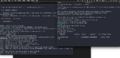
[[File:DIF AT FLASH SETTINGS.png|thumb|T48 programmer settings and dump - note the very interesting strings!]]I used a T48 programmer with a 48pin TTSOP to read the NOR Flash firmware contents - | |||
In the image on the right, are the settings needed for a good read. The NOR flash is 16 bit wide, but the CPU is reading it in 8 bit mode (8 bit mode pin is tied low). SHARP LH28F400BVE Parallel NOR Flash 512kb. The chip is from the late 1990s as the device is also, turn of the century 2000s. | |||
Although the strings are legible in the T48 preview, this is because the T48 is re-arranging the byte order automatically. The byte order must be swapped (little endian) in order to correctly view and disassemble the firmware. I found this out after nonsensical strings were seen, without swapping byte order. I tried some 8 bit reads, but this garbled the strings in the T48. | |||
It was clear 16 bit wide was correct, but then byte order needed changing. I used a python script to swap the byte order of the entire dumped firmware file: <syntaxhighlight lang="python3"> | |||
# swap_bytes.py | |||
input_file = "INTEL_HEX_DIF_AT_LH28F400BVE@TSOP48.bin" | |||
output_file = "INTEL_HEX_DIF_AT_LH28F400BVE@TSOP48_byte_swapped.bin" | |||
with open(input_file, "rb") as f: | |||
data = f.read() | |||
= | # Create a new bytearray for swapped data | ||
swapped = bytearray() | |||
# Swap every pair of bytes (i.e., 16-bit words) | |||
for i in range(0, len(data) - 1, 2): | |||
swapped.append(data[i + 1]) # high byte | |||
swapped.append(data[i]) # low byte | |||
# If the file has an odd number of bytes, keep the last one | |||
if len(data) % 2 != 0: | |||
swapped.append(data[-1]) | |||
# Write the output | |||
with open(output_file, "wb") as f: | |||
f.write(swapped) | |||
print(f"✅ Done. Swapped file saved as: {output_file}") | |||
</syntaxhighlight>The strings are very interesting indeed. Not just a standard 'version' or 'release date' string - they are command strings! | |||
As this device has no screen, a low level diagnostic routine is inferred from their discovery. (though actually, there are also a couple of strings that are sent out via a User Operation, to a device with a screen) Looking closely at the last string or two, I was worried that it might be corrupted as there are some missing letters in the string - (ADAT Sync port di onnected and Dectected rather than Detected). | |||
===Binwalk | ==Examine Firmware -== | ||
I slowed down a bit here because I had no idea how to actually load the file I'd dumped to | ===Binwalk -=== | ||
I slowed down a bit here because I had no idea how to actually load the file I'd dumped to examine it. | |||
First I used [https://github.com/ReFirmLabs/binwalk Binwalk], which I *think* is more suited to SOC work (at least, I think Binwalk is able to find files and systems within bin images, which this firmware does not contain) Anyway Binwalk was able to provide an informative image showing the entropy of the file - low entropy = low chance of corruption or encryption. | |||
I also had a look at [https://binvis.io/ Binvis]. Binvis makes for a stunning visual representation, regardless of anything else at all. I love it. It was fun to see the strings represented in coloured pixels. Also, very apparent to see in Binvis, are the banks. | ===Binvis -=== | ||
I also had a look at [https://binvis.io/ Binvis]. Binvis makes for a stunning visual representation, regardless of anything else at all. I love it. It was fun to see the strings represented in coloured pixels. Also, very apparent to see in Binvis, are the firmware banks. [[File:DIF-AT BINVIS.png|alt=binvis.io|thumb|BINVIS The little 'white line defined' area is where the pointer is viewing]][[File:Binwalk entropy image.png|thumb|Binwalk entropy image looking good - encouraging at least|alt=|none]] | |||
===Firmware Banks -=== | |||
This firmware is banked and split. This is to facilitate DFU - the device can be firmware updated by the user while still maintaining stable OS. Then switch a flag to change/denote active bank. | |||
This device has two firmware version strings visible in the firmware (at this point the strings are the only thing I've been able to see) | This device has two firmware version strings visible in the firmware (at this point the strings are the only thing I've been able to see) | ||
Appears it was already updated in the field to the last OS version (1.022) from I'm not sure if it then wipes the other bank? Possibly, because the other regions are written with FF. However it was still pretty confusing to navigate around later on; BRA from active code to 0xFF region. | Appears it was already updated in the field to the last OS version (1.022) from I'm not sure if it then wipes the other bank? Possibly, because the other regions are written with FF. However it was still pretty confusing to navigate around later on; BRA from active code to 0xFF region. | ||
Probably some of these are the as yet un-mapped SRAM, and Alesis IC addresses. I've added peripheral mapping for the SCI. I'm learning a lot as I go! Also maybe the Alesis ASIC remaps certain memory addresses at run time? (more research has shown that this is likely). These images show the mirrored banked addresses - some lead to empty regions (maybe ram?) and some have near identical code (version differences?) and some have different data (bytes table for strings). [[File:DIF-ATBanked ROM2.png.png|thumb|DIF-AT firmware showing mirrored 'blank' bank location. |alt=]][[File:DIFAT Bank Example.png|alt=DIF-AT firmware with mirrored bank -near identical addressing much higher in ROM region|thumb|DIF-AT firmware with mirrored bank - almost identical addressing just much higher in ROM region|none]] | |||
== | ==Firmware Strings -== | ||
{| class="wikitable sortable" | {| class="wikitable sortable" | ||
|+ | |+ | ||
| Line 224: | Line 243: | ||
| | | | ||
|} | |} | ||
I removed all the strings returned which are over n6 | |||
===Strings -=== | |||
Alright we've heard enough about them; above is the list created with | |||
'''''strings -n 6 INTEL_HEX_DIF_AT_LH28F400BVE@TSOP48_byte_swapped.bin''''' | |||
I removed all the strings returned which are over n6 though not really strings - and - There are also two blank strings which the above table has optimised away. These blank strings seem to have a function, which is unclear at present. | |||
You can see how, it does look like corruption in some of the strings - gaps in the text. | You can see how, it does look like corruption in some of the strings - gaps in the text. | ||
The **Roland xx looks like a boot banner and is called differently in the firmware. I'm sure that's why it has different start and stop markers. Ditto for the early Version string. Interestingly, the early Version is way at the other end of the addresses in the code. This adds to the DFU / Bank swap theory. | The '''**Roland xx''' looks like a boot banner and is called differently in the firmware. I'm sure that's why it has different start and stop markers. Ditto for the early Version string. Interestingly, the early Version is way at the other end of the addresses in the code. This adds to the DFU / Bank swap theory. | ||
When I finally load the firmware (I still haven't at this point) I spend ages looking for what calls these strings. I find it difficult to navigate but fascinating. It is difficult to navigate any production firmware disassembly I expect. I have no prior experience, but it seems the H8300H is kind of a different level, a bit of an oddity. It's used a lot in Japanese electronics | When I finally load the firmware (I still haven't at this point) I spend ages looking for what calls these strings. I find it difficult to navigate but fascinating. It is difficult to navigate any production firmware disassembly I expect. I have no prior experience, but it seems the H8300H is kind of a different level, a bit of an oddity. It's used a lot in Japanese electronics. It is in a lot of Roland devices. Apparently it interleaves code and data frequently which makes static disassembly trickier. ''Especially in Cutter, which won't decompile H8 instructions.'' | ||
===User / Diagnostic Monitor Strings -=== | |||
One or two strings can be discovered, which have a different call system to the diagnostic strings (the ones I'm most interested in) especially because I have to repair so many subsystems, ICs, and traces. | One or two strings can be discovered, which have a different call system to the diagnostic strings (the ones I'm most interested in) especially because I have to repair so many subsystems, ICs, and traces. | ||
I don't know at this point that these diagnostic strings are highly likely to be called by the Monitor Version 1.00, which is highly likely a Machine Language diagnostic tool which must operate over UART. | I don't know at this point that these diagnostic strings are highly likely to be called by the Monitor Version 1.00, which is highly likely a Machine Language diagnostic tool which must operate over UART. | ||
===Video Sync Pal/NTSC Strings -=== | |||
This is an interesting one. The DIF-AT syncing to video?! | |||
Probably the ADAT and TASCAM tape machines, will have a video sync input. Used to sync video gear and score music for TV / video productions, the DIF-AT sees the 'passed through' video sync from the ADAT or the TASCAM. It's not possible to sync the DIF-AT to video without it coming from a tape machine. I'm sure the manual for an ADAT machine will have this info. If I locate the info I will update this section. | |||
==Firmware Disassembly -== | |||
===High Performance Embedded Workshop -=== | ===High Performance Embedded Workshop -=== | ||
[[File:HEW.png|thumb|High Performance Embedded Workshop]] | [[File:HEW.png|thumb|High Performance Embedded Workshop]] | ||
I downloaded HEW from Renesas, which still keeps this available online. Superannuated Software, total 1998 vibes (though I think its 2003) I love that look though! I managed to load the firmware into it, and yes, it appears to be recognised and loads in just fine. This is a big step, its the first time I'm looking at the disassembly, and it seems like its not badly corrupted (it loads it in) I enter the RAM addresses and sizes and mess about with it for a bit. . . | I downloaded HEW from Renesas, which still keeps this available online. Superannuated Software, total 1998 vibes (though I think its 2003) I love that look though! I managed to load the firmware into it, and yes, it appears to be recognised and loads in just fine. This is a big step, its the first time I'm looking at the disassembly, and it seems like its not badly corrupted (it loads it in) I enter the RAM addresses and sizes and mess about with it for a bit. . . | ||
| Line 247: | Line 278: | ||
There was actually some DOS software that I had a crack at too which apparently loaded H8 firmware but I never got it to open the file. | There was actually some DOS software that I had a crack at too which apparently loaded H8 firmware but I never got it to open the file. | ||
==Ghidra -== | ===Ghidra -=== | ||
I find Ghidra and compile Dev version for some reason I can't recall. I think so I | I find Ghidra and compile Dev version for some reason I can't recall. I think so I could load third party CPUs. | ||
'''H8300H is not supported in Ghidra'''. I find a plugin, https://github.com/shizmob/ghidra-h8-300 and try to compile that and load in Ghidra. It won't compile though - Later I also tried https://github.com/carllom/sleigh-h8 which I also don't get running in Ghidra - | |||
I have since managed to compile the H8300H plugin for Ghidra from [https://github.com/carllom/sleigh-h8 carllom]. It seems working well. I just wasn't really au fait enough with compiling using Sleigh a few months ago. It is actually very easy to compile the advanced model, using this repo. | |||
===Cutter -=== | |||
[[File:DIFAT CUTTER SSHOT.png|thumb|DIF-AT firmware loaded into Cutter]] | |||
Cutter was much more useful for what I wanted. Lots of functions were discovered and named with the help of LLMs. (as such, we can't take them as absolutely true, though they are likely to be mostly correct). I was digging around in it for a long time, really interesting - I discovered: | |||
== | ==Discovered Routines -== | ||
=== | ===Diagnostic Routine -=== | ||
Firmware checks for input (button push) in early boot. This branches into and launches diagnostic (Monitor) mode. I think that, after looking at it more: the device will start the tests automatically, when it enters diagnostic mode, and that the strings are an output flag. I don't think the tests are commanded with byte input. It seems firmware is checking for a hardware flag and, depending on value, reports NG or OK. I have to check this when I have the device on the bench. | |||
=== Show Version Routine - === | ===DFU Routine -=== | ||
DFU routine and bytes compared to trigger DFU over midi. Firmware is checking for a series of bytes sent from a different machine - these are user operations not part of diagnostic branch. (''Probable'') '''''DFU mode trigger (multi-byte pattern): AE E8 6A F7''''' | |||
===Show Version Routine -=== | |||
Show version routine. Again a user operation via a different machine. The User sets a byte sequence using a button combo on a Roland mixer. It sends the bytes to the DIF-AT, and it responds by printing the DIF-AT Version number over midi, on the mixer display screen. | Show version routine. Again a user operation via a different machine. The User sets a byte sequence using a button combo on a Roland mixer. It sends the bytes to the DIF-AT, and it responds by printing the DIF-AT Version number over midi, on the mixer display screen. | ||
These operations are described below. I found them on Roland's site, and then looked for the relevant part of the firmware which checks for these bytes. '''''Send single byte 0x06 from host to device. That causes the device to: enter Show-Version handler run fcn.ShowVersionSequence() transmit the version bytes to host. return to idle mode''''' | These operations are described below. I found them on Roland's site, and then looked for the relevant part of the firmware which checks for these bytes. Notes from examining the firmware - '''''Send single byte 0x06 from host to device. That causes the device to: enter Show-Version handler run fcn.ShowVersionSequence() transmit the version bytes to host. return to idle mode''''' | ||
{| class="wikitable" | {| class="wikitable" | ||
|+ | |+ | ||
| Line 333: | Line 370: | ||
|} | |} | ||
=== Firmware Update Files - === | ==Firmware Updating / Appropriating -== | ||
===Firmware Update Files -=== | |||
The firmware itself is ''still'' available from Roland, as midi update files. These files are sent to the DIF-AT over its RBUS midi port, from an RBUS capable device. (Although classic Roland it seems to be only ''one'' digital mixer that has the correct button sequence to do the update / show version) However Roland are correct in that a user needs an RBUS port to send the midi files, as the DIF-AT midi port is two pins on the RBUS connector. | |||
https://www.roland.com/us/support/by_product/dif-at/updates_drivers/ac2a8693-f923-4894-9d8d-da20af3b75ef/ (mac, sea.hqx) | https://www.roland.com/us/support/by_product/dif-at/updates_drivers/ac2a8693-f923-4894-9d8d-da20af3b75ef/ (mac, sea.hqx) | ||
| Line 340: | Line 379: | ||
https://www.roland.com/us/support/by_product/dif-at/updates_drivers/86187843-8227-4307-b9f5-246ffcc7e27f/ (windows) | https://www.roland.com/us/support/by_product/dif-at/updates_drivers/86187843-8227-4307-b9f5-246ffcc7e27f/ (windows) | ||
I have not yet performed a Diff of my firmware and the midi updates. I would have to reconstruct them first into a full image. I think my firmware is not corrupted though at this point. I will try and send the DFU command and the payload using a python script instead: | I have not yet performed a Diff of my firmware and the midi updates. I would have to reconstruct them first into a full image. I think my firmware is not corrupted though at this point. I will try and send the DFU command and the payload using a python script instead (see below) | ||
The midi files are 4x33kb. Minus headers etc; 32kb actual payload x 4 = 128kb firmware. A 512kb NOR flash is generous space for this (4x bigger) Though remember its banked for DFU (when the update is written and verified it will switch active bank flag) Also it seems remapped to different addresses in runtime operation also. | |||
If anyone has tips on how to separate the two banks in the full dump of firmware, please let me know. I expect it is as we can see, the earlier version string response is in the earlier version firmware bank and vice versa. Though it is still not really clear where the lines diverge! | |||
===DFU Python Script=== | |||
With more help from LLM I made a DFU Update python script which first sends the (probable) DFU command, and then sends sequentially all midi files over serial (at midi baud) I compared the received payload to the sent, and it is correct. I have yet to test on the device.<syntaxhighlight lang="python3"> | |||
import serial | |||
import time | |||
from pathlib import Path | |||
# ========================= | |||
# CONFIGURATION | |||
# ========================= | |||
UART_PORT = 'socket://192.168.1.182:31250' # ser2net using raw TCP | |||
BAUD_RATE = 31250 # MIDI baud | |||
DFU_TRIGGER = bytes([0xAE, 0xE8, 0x6A, 0xF7]) | |||
FILES_TO_SEND = [ | |||
'difsys1.mid', | |||
'difsys2.mid', | |||
'difsys3.mid', | |||
'difsys4.mid' | |||
] | |||
PAUSE_BETWEEN_FILES = 1.5 # seconds | |||
BYTE_DELAY = 0.00032 # per byte (~320 µs) | |||
DFU_DELAY = 1 # seconds to wait after sending trigger | |||
# ========================= | |||
# HELPER FUNCTIONS | |||
# ========================= | |||
def send_file(uart, filepath): | |||
filepath = Path(filepath) | |||
if not filepath.is_file(): | |||
print(f"⚠️ File not found: {filepath}") | |||
return False | |||
filesize = filepath.stat().st_size | |||
print(f"📤 Streaming {filepath} ({filesize} bytes)...") | |||
sent_bytes = 0 | |||
with filepath.open('rb') as f: | |||
while (byte := f.read(1)): | |||
uart.write(byte) | |||
sent_bytes += 1 | |||
if BYTE_DELAY > 0: | |||
time.sleep(BYTE_DELAY) | |||
if sent_bytes % 1024 == 0 or sent_bytes == filesize: | |||
pct = (sent_bytes / filesize) * 100 | |||
print(f"\rProgress: {pct:.1f}%", end='', flush=True) | |||
print("\rProgress: 100.0% ✅") | |||
return True | |||
# ========================= | |||
# MAIN ROUTINE | |||
# ========================= | |||
def main(): | |||
try: | |||
uart = serial.serial_for_url( | |||
UART_PORT, | |||
baudrate=BAUD_RATE, | |||
bytesize=serial.EIGHTBITS, | |||
parity=serial.PARITY_NONE, | |||
stopbits=serial.STOPBITS_ONE, | |||
timeout=0.1 | |||
) | |||
print(f"Opened UART on {UART_PORT} at {BAUD_RATE} bps.") | |||
time.sleep(4.0) # allow connection to fully settle | |||
uart.reset_input_buffer() | |||
uart.reset_output_buffer() | |||
print("UART ready — flushing done, waiting 4s before sending DFU trigger...") | |||
except Exception as e: | |||
print(f"❌ Failed to open UART: {e}") | |||
return | |||
# --- DFU Trigger --- | |||
print(f"Sending DFU trigger: {DFU_TRIGGER.hex()}") | |||
uart.write(DFU_TRIGGER) | |||
uart.flush() | |||
time.sleep(DFU_DELAY) | |||
# --- Stream Update Files --- | |||
for file_path in FILES_TO_SEND: | |||
if not send_file(uart, file_path): | |||
print("❌ Aborting: file not found or error.") | |||
break | |||
time.sleep(PAUSE_BETWEEN_FILES) | |||
uart.close() | |||
print("🎉 All files streamed successfully.") | |||
if __name__ == "__main__": | |||
main() | |||
</syntaxhighlight><syntaxhighlight lang="python"> | |||
readme python dfu update - | |||
1 Put your MIDI files in the same folder as the script | |||
Name them exactly as in the script, or update FILES_TO_SEND in the script to match your filenames: | |||
FILES_TO_SEND = [ | |||
'update1.mid', | |||
'update2.mid', | |||
'update3.mid', | |||
'update4.mid' | |||
] | |||
2 Adjust the UART port | |||
Set UART_PORT in the script to your actual port: | |||
Windows: COM3, COM4, etc. | |||
Linux/Mac: /dev/ttyUSB0, /dev/tty.usbserial-XXXX, etc. | |||
UART_PORT = 'COM3' | |||
3 Run the script | |||
Open a terminal/command prompt in the folder with the script and MIDI files: | |||
python your_script_name.py | |||
You should see: | |||
Opened UART on COM3 at 31250 bps. | |||
Sending DFU trigger command... | |||
Streaming update1.mid (12345 bytes)... | |||
Progress: 100.0% | |||
Finished streaming update1.mid | |||
Streaming update2.mid ... | |||
... | |||
All files streamed successfully. | |||
⚡ Notes | |||
Make sure nothing else is using the UART port while running the script. | |||
The BYTE_DELAY = 0.00035 handles average 120 BPM playback, no per-file analysis needed. | |||
If a file is missing, the script will print an error and stop. | |||
</syntaxhighlight> | |||
===Misappropriate Firmware -=== | |||
I've been thinking: "how would I get the firmware off the flash, with no access to a programmer or firmware files?" | |||
There is only a boot-loader (no JTAG or SWD) and the chip is fixed in boot mode with pins, and also, there is no firmware stored on the cpu! Attack vector would have to be: Take control of the bus, and write the firmware a byte at a time out with an MCU (pi pico, arduino, teensy) | |||
If the device was sent into Show Version Mode, it accesses flash to read version and then send over UART to external device. | |||
After this (according to Roland's notes) the device must be powered off and rebooted, to return to normal boot mode: | |||
'''''ie''''' - stays in an idle or wait / sleep loop. | |||
I'm sure that it's not accessing flash after the version string is collected. (though this could easily be checked with a scope or LA) | |||
This is probably the ideal time to use the 50 pin header for an attack. Send a manual BREQ bus request (pull BREQ low); thus taking control of the flash access from the Bus Arbitrator (Alesis IC). As long as WE# and CE# are low (they should be if bus access is granted, though they could also be held low in case something woke up). Again this could easily be determined by entering the Show Ver. routine and looking at the pin activity. Sure it's possible. | |||
<br /> | |||
==Digital Audio Formats -== | |||
===Roland RBUS -=== | |||
Here I will refer to the excellent site of Chris Xiong who made a converter from RBUS>ADAT (but not bi-directional) He covers the technical aspect of the RBUS signal and pinouts etc here in detail - | |||
https://chrisoft.org/blog/post/2024-02-02.html (RBUS technical information) | |||
https://chrisoft.org/blog/post/rbus-adat-m.html (Project page) | |||
[[File:DIF AT RBUS CONNECTOR SCHEMATIC.png|alt=RBUS - Connector schematic|thumb|RBUS - Connector schematic]] | |||
From the VS2480 service manual we can see this schematic about the RBUS connector - it is a bi-directional transfer (audio in and audio out) so it crosses over (like a null modem cable) | |||
===Tascam T-DIF -=== | |||
I didn't go much into the TDIF as I don't have anything TDIF capable. Both RBUS and TDIF are long obsolete, but ADAT is still going strong. A pinout of the TDIF connector is shown here: | |||
https://www.panix.com/~jens/da-88/tdif.html | |||
TDIF uses balanced connections, it is a more professional format. Tascam digital dsub connection is now a standard. It is different to TDIF, though has its origins there. | |||
https://en.wikipedia.org/wiki/Tascam_Digital_Interface | |||
Tascam also made a, more professional, converter box: the IF TAD https://www.tascam.eu/en/docs/IF-TAD_manual.pdf | |||
However this is only between TDIF and ADAT. | |||
===Alesis ADAT -=== | |||
https://www.vintagedigital.com.au/alesis-adat/ | |||
https://www.gearnews.com/the-history-of-adat-how-alesis-changed-digital-recording/ | |||
Nice write ups here with lots of details. I use optical ADAT. There is no pinout to mention. DIF-AT uses TORX connectors, which are now obsolete. The connectors been modernised with a spring door to keep out dust. The original have removable dust caps which are invariably lost over time.<br /> | |||
==Repairs -== | |||
Flashed the firmware onto a new NOR flash chip. SRAM replaced (these are almost a consumable) I have had one of this range fail before, in a different package. Not ahead of time, but yeah it failed. | |||
Other ICs were replaced (including CPU) Traces repaired (almost 20) Most of which surrounding CPU. | |||
Leg of a custom Alesis IC was repaired (there are three custom Alesis chips, two small one large). This 8 pin chip was bridged vcc/gnd with a capacitor (factory modification). Removing the cap, broke the leg off the IC. I was able to grind away the epoxy and solder a new leg in place. | |||
All the pins on the 100 pin Xilinx and 100 pin Alesis IC were reflowed and any other flaky looking connections. | |||
The LED legs had metal fatigued off with all the repairs. I ground away the solder resist and was able to solder them directly to the board again. LEDs are a custom design package. Also, its best to use the original: only the legs were broken after all.<gallery> | |||
File:Dif-at-tracerepair.png|alt=Traces replaced and connected.|Traces replaced and connected. | |||
File:Dif-at-tracerepair2.png|traces tinned (way too much, I took some off with wick) | |||
File:Dif-at-tracerepair3.png|placing component | |||
File:Dif-at-tracerepair4.png|CPU traces repaired. Sorry, not a great shot | |||
</gallery> | |||
==To Do -== | |||
1 - Test device first real power on. | |||
2 - Logic Capture 50 pin header signals. | |||
3 - Use UART Monitor program to run diagnostic commands. | |||
4 - Investigate nature of Alesis chip. | |||
5 - Update this wiki with final findings. | |||
After some months working on this, and seeing the LEDs blink again (it took an embarrassingly long time to realise they were pulled high) I was satisfied I could take a short break from it. I will complete the repair by fully testing it and running the UART Monitor program. | |||
A deeper look at the Alesis chip: It is possible that it is a pre-programmed CPLD, but that it has JTAG access. More likely it's an ASIC rather than OTP CPLD or GAL, PAL. Still though, it would be interesting to reveal something about it. As I said it's not on the JTAG chain here anyway. | |||
I will update this when the device is fully tested. For now, be assured that it's back together, repaired, and starting to boot. There could be some small issues, which can be discovered and fixed with the UART function. I could only continue the marathon with a reboot myself. | |||
Thanks for reading. I hope it's interesting and or useful! If you want the Cutter project file I can send it you, email me through the site. Or any questions I'd be happy to answer. | |||
Below are some general pinout notes on the DIF-AT RBUS and Digital Audio flow, and the connections to the Alesis Chip (which seems to do all the heavy lifting as regards audio and timing) | |||
All audio formats go directly into the Alesis chip, and it handles so much, audio formats, inputs, - BREQ bus arbitration, WE to Flash, CE with mux to Flash, that it must be an ASIC. Any thoughts on this, or anything else here, are most welcome. | |||
The Xilinx chip is handling RBUS signals only, after they leave the Alesis chip, they go into the Xilinx CPLD, and leave the DIF AT via an inverter. I will inspect the signals before and after the Xilinx cpld to see how it is processing the data. | |||
<br /> | |||
==NOTES -== | |||
Xilinx CPLD solely handles r-bus output signals, taking from Alexis, re-timing/re -serialising? then output - 4 in 4 out (stereo pairs 8 channel audio) | |||
Alesis chip handles all format inputs and outputs them (retiming/prioritising?) | |||
Cpu 8 - tif con pb / tp/ txd 2 CPU (seems to communicate with serial to TDIF board) | |||
Cpu 9 - tif con pb / tp/ rxd2 CPU (seems to communicate with serial to TDIF board) | |||
UART serial output - | |||
From cpu 12 - txd0 - uart, midi baud | |||
to Pin 13 ic 29 (inverter) 2a2 - output pin 7 2y2 | |||
Then via (not thru) diode/ resistor to | |||
Pin 14 R-BUS CONN. RBUS_TX (MIDI transmit) | |||
(In r-bus cable this crosses over to ARRIVE AT MIDI receive ON RECIPIENT DEVICE) | |||
Cpu 13 out (txd1) ic 11 - sync signal? | |||
Cpu 16 Sck0 irq4 or p94 | |||
Goes to T Dif con | |||
Cpu 17 - sck1 irq5 p95 | |||
Goes to ic 29 pin 3 (2Y - output, inverted) | |||
Input = 2a, pin 17 - ????? | |||
Pin 25 R-BUS CONN. RBUS_RX (MIDI receive) | |||
via (not thru) diode/ resistor TO pin 13 a6 ic 27 (INVERTER input) | |||
Output pin 12 y6 - to pin 14 cpu RX0 UART RECEIVE SIGNAL - | |||
PIN 13 R-BUS CONN. Power reception for bus-powered devices | |||
This is where power comes into the Dif at - directly into the large filter capacitor. | |||
(Routed from pin 5 of the r-bus connector via crossover cable) | |||
Pin 21 R-BUS CONN. Frame sync (word clock) input | |||
to Pin 15 input (inverter) ic 29 2a3 - output 2y3 pin 5- | |||
then to pin 6,10,11,12 on ic 28 (muxer) | |||
(Investigate further where does it leave MUXER?) cpu or cpld?' | |||
Pin 18 R-BUS CONN. Frame sync (word clock) output | |||
to Pin 11 input (inverter) ic 29 2a1 - output 2y1 pin 9 - | |||
then to pin 7 on ic 28 (muxer) also pin 93 tp0 cpu (programmable timer, like tp3) | |||
and last pin on cn6 to tif board (not pin1!) | |||
R-bus inputs - | |||
Pin 12 R-BUS CONN. Channel 1/2 input (SDIN1) | |||
Via resistor + via diode to Pin 11 a5 (input inverter) ic 27 - output pin 10 y5 | |||
To pin 49 Alexis cpld (data input) | |||
Pin 11 R-BUS CONN. Channel 3/4 input (SDIN2) | |||
Via resistor + via diode to Pin 9 a4 (input inverter) ic 27 - output pin 8 y4 | |||
To pin 48 Alexis cpld (data input) | |||
Pin 10 R-BUS CONN. Channel 5/6 input (SDIN3) | |||
Via resistor + via diode to Pin 5 a3 (input inverter) ic 27 - output pin 6 y3 | |||
To pin 47 Alexis cpld (data input) | |||
Pin 8 R-BUS CONN. Channel 7/8 input (SDIN4) | |||
Via resistor + via diode to Pin 3 a2 (input inverter) ic 27 - output pin 4 y2 | |||
To pin 46 Alexis cpld (data input) | |||
[R-Bus is then internal, along with a-dat and t-dif, they are translated into each other by the cpld] | |||
Internal r-bus - | |||
Alesis cpld pin 57 (data output) to Xilinx pin 45 (data input) | |||
Alesis cpld pin 56 (data output) to Xilinx pin 44 (data input) | |||
Alesis cpld pin 55 (data output) to Xilinx pin 43 (data input) | |||
Alesis cpld pin 52 (data output) to Xilinx pin 42 (data input) | |||
(three pins are consecutive, then a gap) | |||
Flows to - | |||
R-bus outputs - | |||
Pin 55 Xilinx - (data output) | |||
To pin 8 ic 29 (1a4) inverter / output pin 12 (1y4) then | |||
thru ESD diode + resistor path to Pin 2 R-BUS CONN. Channel 1/2 output (SDOUT1) | |||
Pin 56 Xilinx - (data output) | |||
To pin 6 ic 29 (1a3) inverter / output pin 14 (1y3) then | |||
thru ESD diode + resistor path to Pin 3 R-BUS CONN. Channel 3/4 output (SDOUT2) | |||
Pin 57 Xilinx - (data output) | |||
To pin 4 ic 29 (1a2) inverter / output pin 16 (1y2) | |||
thru ESD diode + resistor path | |||
to Pin 4 R-BUS CONN. Channel 5/6 output (SDOUT3) | |||
Pin - 58 Xilinx - (data output) | |||
to pin 2 ic 29 (1a1) (inverter) output Pin 18 -(1y1) | |||
thru ESD diode + resistor path to pin 6 R-BUS CONN. Channel 7/8 output (SDOUT4) | |||
Alesis pin 63 (input) = adat optical input (from Torx conn) | |||
Alesis pin 62 (output) = adat optical output (from Torx conn) | |||
Alesis pin 64 (input) = adat sync chip ic8 pin 7 (output?) | |||
Alesis pin 60 (input) = adat sync chip ic10 pin 7 (output?) | |||
<nowiki>'''''''''''''''''''''''''''''''</nowiki> | |||
Ic 18 (opto-isolator) - | |||
Ic 16 (opto-isolator) - to Ic 28 (multiple pins, bridged) (mux)'<nowiki/>'''<nowiki>'''''</nowiki>'''''<nowiki>'''''</nowiki>'' | |||
Ic 14 (opto-isolator) - to Alesis cpld pin 58 | |||
Ic 12 (opto-isolator) - to cpu pin 15 (rx1 SERIALinput) | |||
Pin 1 - t Dif = pin 18 ya1 buffer = - input 1a1 pin 2 - pin 6 ff conn (t Dif pcb) - pin 6 cn6 main board. | |||
Ic 9 pin 1 1a (inverter input) x2 (crystal) output via r63 | |||
Clock pin Alesis cpld pin 75 - ic 9 pin pin 7 1y (inverted output) + ic 15 pin 13 | |||
<nowiki>''''''''''''''''''</nowiki> | |||
Ic 9 pin 3 2a (inverter input) to ic 13 (4066) pin 12 (ctl-d - d-11/10) ALSO to BREQ CPU 59 (PULLED HIGH ALSO) | |||
+ ic 17 (dual bus buffer) pin 1, 7 (high impedance state [input] control pins) | |||
Ic 9 pin 5 2y (inverter output) to ic 11 (octal Buffer) pins 1, 19 (TRI_STATE ENABLE, A+B) + ic 13 (4066), pins 5,6,13 (control pins b,C,A) | |||
Ic 9 pin 6 3a (inverter input) to | |||
Ic 9 pin 2 3y (inverter output) to ???? Can't find yet!!!!! (INPUT not tied to gnd or high so must be valid input) | |||
Breq seems to be tied into the sync master ports, which system is syncing - tsdif adat. | |||
Alesis pin 1 to 24 connects to flash + sram. | |||
Latest revision as of 12:17, 10 May 2026
PCB photos, Pinouts, Pin header, Device operation, Connections between subsystems. Notes on firmware structure, Machine language monitor program, DFU, firmware extraction, firmware update script (python)

Brief outline -
I bought this device to repair. They are rare, and interesting. It would not respond any longer or be recognised by host hardware. (it runs in conjunction with host digital mixer / host music production device, translating digital audio formats in real time)
I damaged a lot of traces on the device and gave up on it. However, I learned how to micro-solder and became inspired to continue the repair with reverse engineering techniques. This is my first reverse engineering project, though I have worked on modding and repairing before.
Given the device was already non-responsive (and now damaged further) -
Goals-
- De-solder NOR Flash and read firmware.
- Determine potential corruption of firmware.
- Re-flash firmware onto new NOR flash (if good).
- Determine operation / corruption of Xilinx CPLD/Alesis IC - read contents.
- Analyse firmware for anything interesting.
- Determine and examine / analyse hardware architecture.
- Repair traces, replace ICs. Test.
- Collate information, share research and findings.
PCB Photos -
-
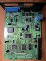 Main board
 -
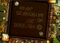
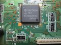 Cpu (not mcu!)
 -
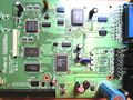 Main board, alt
 -
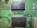 SRAM + NOR Flash (512kb)
 -
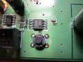
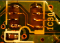
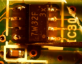
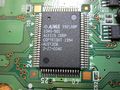 Custom Alesis chip OTP CPLD? GAL?
 -
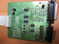 TDIF daughter board
 -
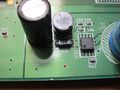 5v power conditioning
 -
 Sync circuitry with optocouplers
 -
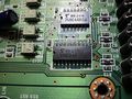
 Reset IC and switch
 -
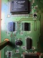 Xilinx CPLD with JTAG pads visible (pin 50, 81 silkscreen)


Device Overview
This is a complex device with a 16 bit CPU, Xilinx 95xx CPLD, Custom Alesis chip (ASIC, Gate array, PAL, GAL, OTP CPLD?) SRAM, NOR flash 512kb, logic and switching for bus arbitration. BREQ Bus request is a very involved circuit. Also CE# Chip Enable NOR Flash is connected through a complicated muxing circuit. The Alesis custom IC handles the WE# Write Enable to the NOR Flash, and also seems BREQ master.
No info could be found on the Alesis chip, searching for the numerous IC markings revealed nothing. After more research, it seems likely it is an ASIC, as the functions it performs are advanced.
The Device is quite old school. This was built for the early generation of ADAT/TDIF machines, still using physical tape. Thankfully a tape machine is not necessary for operation. The sync requirements of locking digital audio using analogue tape definitely adds complexity to this system.
Device has 2 buttons on the PCB: Switch 1 - RESET, reset circuit (dedicated IC) Switch 2 - Launch monitor diagnostic mode.
A 50 pin header provides easy access to most address lines and relevant (to operation) CPU/RAM/Flash lines. This will be convenient to run a logic capture during boot and operation later. I beeped out the 50 pin connector - Many pins have multiple connections. Happily; the vias were not tented - this was a long endeavour even with continuity through the vias : ) Below, the findings and some general notes:
-
 Header pins 1 - 16
 -
 Header pins 16 - 24
 -
 Header pins 15 to 38
 -
 Header pins 38 to 50
 -
 General notes about inferred operation


JTAG/Programming/CPLD
The device has two levels of firmware: NOR Flash and CPLD bitstream. The Xilinx is an older model XC95144 which is programmed over JTAG. However (as I understand it) due to the architecture: bitstream cannot be read out over JTAG (even if unlocked) It has to use vendor specific tools (Platform Cable USB) in order to recover the bitstream.
JTAG pads are exposed on the PCB as seen in the image above. I could connect to these to read the CPLD. Pretty soon they were pulled off the board, and I had to solder a pin to the leg temporarily to continue reading data. (before I discovered tiny IC clips!)
[Only one device is visible in the JTAG chain, the Xilinx. The CPU, H8300H (Hitachi/Renesas) is not equipped with JTAG at all. Low level CPU operation is done through a bootloader mode] Interesting and lovely late 1990s marketing publication here
I connected to the Xilinx XC95144 using Bluetag, OpenOCD and XC3SPROG (open source Xilinx CLI) and was eventually able to read back ID codes and find IR Len etc. I was happy it was responding. It was fun, confusing and difficult to set up all these tools. I set most of them up on a Raspberry Pi as dedicated hacking server so I can connect remotely to the hot mess setup with my laptop, somewhere more comfortable : )
It seems strange to me that, this is a 100 pin CPLD, and only 4 inputs and 4 outputs are used! (solely RBUS data, 8 channels L/R in/out). Counter output from H8300H goes to clock pin of the Xilinx, through an inverter.
-
 XC3SPROG id read
 -
 Pullup info from Xilinx
 -
 BlueTag correctly reads pins
 -
 OpenOCD and BlueTag (in BusPirate Mode)


BSDL Scan -

After initial ID code read, I used a BSDL GUI to determine whether the CPLD was actually passing data throughput. Whilst easy to use when running, this tool took a while to set up (I mistakenly compiled it from source in Windows 7 32 bit - somehow missing the fact there there was a package release) After downloading the BSDL language file from Xilinx and setting up the tool with info from the Xilinx datasheet (super confusing naming convention, cells vs physical pins). Scanner could only run with this set up in Extest mode (OS not present nor running) toggling the input pins at a user defined frequency - means the corresponding output logic pulses accordingly.
It was satisfying to see my logic probe light up on the outputs during Extest scanning.
Xilinx CPLD confirmed working - big achievement! (Not tested in actual operation) I'm 99% sure its fine after these tests.
At some point I will get a Xilinx Platform Cable to attempt to read the bitstream for archival purposes. However at this stage I'd had to get a few probes etc and didn't really want to get a Xilinx only device. I've had great luck with unlocked devices so far though, everything I've looked at has been open or level 1 : )
Extract Flash Firmware -
At some point in the repair attempt, I heard a strange flapping sound from the NOR Flash as I moved the device around. ALL of the pins 25 - 48 had detached from the PCB with zero damage to the traces or pins. I surmise that this was the original failure point of the device - dry joints on the Flash chip. After I desoldered the other half using hot air, I could proceed to read out the contents -
T48 Programmer-

I used a T48 programmer with a 48pin TTSOP to read the NOR Flash firmware contents -
In the image on the right, are the settings needed for a good read. The NOR flash is 16 bit wide, but the CPU is reading it in 8 bit mode (8 bit mode pin is tied low). SHARP LH28F400BVE Parallel NOR Flash 512kb. The chip is from the late 1990s as the device is also, turn of the century 2000s.
Although the strings are legible in the T48 preview, this is because the T48 is re-arranging the byte order automatically. The byte order must be swapped (little endian) in order to correctly view and disassemble the firmware. I found this out after nonsensical strings were seen, without swapping byte order. I tried some 8 bit reads, but this garbled the strings in the T48.
It was clear 16 bit wide was correct, but then byte order needed changing. I used a python script to swap the byte order of the entire dumped firmware file:
# swap_bytes.py

input_file = "INTEL_HEX_DIF_AT_LH28F400BVE@TSOP48.bin"
output_file = "INTEL_HEX_DIF_AT_LH28F400BVE@TSOP48_byte_swapped.bin"

with open(input_file, "rb") as f:
    data = f.read()

# Create a new bytearray for swapped data
swapped = bytearray()

# Swap every pair of bytes (i.e., 16-bit words)
for i in range(0, len(data) - 1, 2):
    swapped.append(data[i + 1])  # high byte
    swapped.append(data[i])      # low byte

# If the file has an odd number of bytes, keep the last one
if len(data) % 2 != 0:
    swapped.append(data[-1])

# Write the output
with open(output_file, "wb") as f:
    f.write(swapped)

print(f"✅ Done. Swapped file saved as: {output_file}")
The strings are very interesting indeed. Not just a standard 'version' or 'release date' string - they are command strings!
As this device has no screen, a low level diagnostic routine is inferred from their discovery. (though actually, there are also a couple of strings that are sent out via a User Operation, to a device with a screen) Looking closely at the last string or two, I was worried that it might be corrupted as there are some missing letters in the string - (ADAT Sync port di onnected and Dectected rather than Detected).
Examine Firmware -
Binwalk -
I slowed down a bit here because I had no idea how to actually load the file I'd dumped to examine it.
First I used Binwalk, which I *think* is more suited to SOC work (at least, I think Binwalk is able to find files and systems within bin images, which this firmware does not contain) Anyway Binwalk was able to provide an informative image showing the entropy of the file - low entropy = low chance of corruption or encryption.
Binvis -
I also had a look at Binvis. Binvis makes for a stunning visual representation, regardless of anything else at all. I love it. It was fun to see the strings represented in coloured pixels. Also, very apparent to see in Binvis, are the firmware banks.


Firmware Banks -
This firmware is banked and split. This is to facilitate DFU - the device can be firmware updated by the user while still maintaining stable OS. Then switch a flag to change/denote active bank.
This device has two firmware version strings visible in the firmware (at this point the strings are the only thing I've been able to see)
Appears it was already updated in the field to the last OS version (1.022) from I'm not sure if it then wipes the other bank? Possibly, because the other regions are written with FF. However it was still pretty confusing to navigate around later on; BRA from active code to 0xFF region.
Probably some of these are the as yet un-mapped SRAM, and Alesis IC addresses. I've added peripheral mapping for the SCI. I'm learning a lot as I go! Also maybe the Alesis ASIC remaps certain memory addresses at run time? (more research has shown that this is likely). These images show the mirrored banked addresses - some lead to empty regions (maybe ram?) and some have near identical code (version differences?) and some have different data (bytes table for strings).


Firmware Strings -
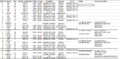
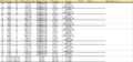
| mpTp**RolandDIF-AT**z
:MONITOR Ver.1.00z mpVp DIF-AT system program Ver 0.9800 H0123456789ABCDEF System Version = Check Sum = 0123456789ABCDEF Flash memory OK. Flash memory check error RAM test OK. RAM test NG. RS-422 loopback test 1 OK. RS-422 loopback test 1 NG. RS-422 loopback test 2 OK. RS-422 loopback test 2 NG. DA-88 sync loopback test 1 OK. DA-88 sync loopback test 1 NG. DA-88 sync opback test 2 OK. DA-88 sync loopback test 2 NG. ADAT sync loopback test 1 OK. ADAT sync loopback test 1 NG. ADAT sync loopback test 2 OK. ADAT sync loopback test 2 NG. RMDB Fs unstable. Video sync in check NG. NTSC video signal received. PAL video signal received. Video signal checked NG. Different sampling Clock. Check the sampling rate. ADAT Sync port di onnect. DA-88 Sync port disconnect. Dectecte tape end. Tape is write pr 0ected. Tape Ejected. Unformat Tape. !"#$%&'()0123456789@ABCDEFGHIPQRSTUVWXY DIF-AT system program Ver 1.022 |
|||
|---|---|---|---|
Strings -
Alright we've heard enough about them; above is the list created with
strings -n 6 INTEL_HEX_DIF_AT_LH28F400BVE@TSOP48_byte_swapped.bin
I removed all the strings returned which are over n6 though not really strings - and - There are also two blank strings which the above table has optimised away. These blank strings seem to have a function, which is unclear at present.
You can see how, it does look like corruption in some of the strings - gaps in the text.
The **Roland xx looks like a boot banner and is called differently in the firmware. I'm sure that's why it has different start and stop markers. Ditto for the early Version string. Interestingly, the early Version is way at the other end of the addresses in the code. This adds to the DFU / Bank swap theory.
When I finally load the firmware (I still haven't at this point) I spend ages looking for what calls these strings. I find it difficult to navigate but fascinating. It is difficult to navigate any production firmware disassembly I expect. I have no prior experience, but it seems the H8300H is kind of a different level, a bit of an oddity. It's used a lot in Japanese electronics. It is in a lot of Roland devices. Apparently it interleaves code and data frequently which makes static disassembly trickier. Especially in Cutter, which won't decompile H8 instructions.
User / Diagnostic Monitor Strings -
One or two strings can be discovered, which have a different call system to the diagnostic strings (the ones I'm most interested in) especially because I have to repair so many subsystems, ICs, and traces.
I don't know at this point that these diagnostic strings are highly likely to be called by the Monitor Version 1.00, which is highly likely a Machine Language diagnostic tool which must operate over UART.
Video Sync Pal/NTSC Strings -
This is an interesting one. The DIF-AT syncing to video?!
Probably the ADAT and TASCAM tape machines, will have a video sync input. Used to sync video gear and score music for TV / video productions, the DIF-AT sees the 'passed through' video sync from the ADAT or the TASCAM. It's not possible to sync the DIF-AT to video without it coming from a tape machine. I'm sure the manual for an ADAT machine will have this info. If I locate the info I will update this section.
Firmware Disassembly -
High Performance Embedded Workshop -

I downloaded HEW from Renesas, which still keeps this available online. Superannuated Software, total 1998 vibes (though I think its 2003) I love that look though! I managed to load the firmware into it, and yes, it appears to be recognised and loads in just fine. This is a big step, its the first time I'm looking at the disassembly, and it seems like its not badly corrupted (it loads it in) I enter the RAM addresses and sizes and mess about with it for a bit. . .
Ultimately, its not great for RE. It was probably good at the time for developing for the H8, but it's pretty hard to use for RE. I give it up.
There was actually some DOS software that I had a crack at too which apparently loaded H8 firmware but I never got it to open the file.
Ghidra -
I find Ghidra and compile Dev version for some reason I can't recall. I think so I could load third party CPUs.
H8300H is not supported in Ghidra. I find a plugin, https://github.com/shizmob/ghidra-h8-300 and try to compile that and load in Ghidra. It won't compile though - Later I also tried https://github.com/carllom/sleigh-h8 which I also don't get running in Ghidra -
I have since managed to compile the H8300H plugin for Ghidra from carllom. It seems working well. I just wasn't really au fait enough with compiling using Sleigh a few months ago. It is actually very easy to compile the advanced model, using this repo.
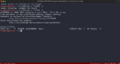
Cutter -

Cutter was much more useful for what I wanted. Lots of functions were discovered and named with the help of LLMs. (as such, we can't take them as absolutely true, though they are likely to be mostly correct). I was digging around in it for a long time, really interesting - I discovered:
Discovered Routines -
Diagnostic Routine -
Firmware checks for input (button push) in early boot. This branches into and launches diagnostic (Monitor) mode. I think that, after looking at it more: the device will start the tests automatically, when it enters diagnostic mode, and that the strings are an output flag. I don't think the tests are commanded with byte input. It seems firmware is checking for a hardware flag and, depending on value, reports NG or OK. I have to check this when I have the device on the bench.
DFU Routine -
DFU routine and bytes compared to trigger DFU over midi. Firmware is checking for a series of bytes sent from a different machine - these are user operations not part of diagnostic branch. (Probable) DFU mode trigger (multi-byte pattern): AE E8 6A F7
Show Version Routine -
Show version routine. Again a user operation via a different machine. The User sets a byte sequence using a button combo on a Roland mixer. It sends the bytes to the DIF-AT, and it responds by printing the DIF-AT Version number over midi, on the mixer display screen.
These operations are described below. I found them on Roland's site, and then looked for the relevant part of the firmware which checks for these bytes. Notes from examining the firmware - Send single byte 0x06 from host to device. That causes the device to: enter Show-Version handler run fcn.ShowVersionSequence() transmit the version bytes to host. return to idle mode
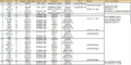
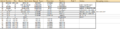
| Updating the DIF-AT from Standard MIDI Files
DIF-AT system software is supplied as 4 files in Standard MIDI File (SMF) format. Tools required: * A product with MIDI In and R-BUS connection, such as the VM-3100Pro (used in this example) * MIDI Sequencer capable of reading and transmitting SMFs with System Exclusive messages * MIDI Cable * R-BUS Cable * System Update files HOW TO UPDATE THE SYSTEM 1) Using R-BUS cable, connect R-BUS terminal of DIF-AT to R-BUS terminal of VM-3100Pro. 2) Using MIDI cable, connect the MIDI OUT of the sequencer to the MIDI IN of the VM-3100Pro. 3) Power on the VM-3100Pro while holding the Channels 6 and 9/10 SELECT buttons. 4) CURSOR to "03:DIF-AT Update," and press ENTER. 5) Load and play the update files from the MIDI Sequencer in order. 6) The ADAT and TASCAM leds will light when the update procedure is completed. 7) Power off and on the VM-3100Pro and the DIF-AT. VERSION CONFIRMATION 1) Using R-BUS cable, connect R-BUS terminal of DIF-AT to R-BUS terminal of VM-3100Pro. 2) Power on the VM-3100Pro while holding the Channels 6 and 9/10 SELECT buttons. 3) CURSOR to "02:DIF-AT Check," and press ENTER. 4) Press F4 to display the system version. 5) Power off and on the VM-3100Pro and the DIF-AT. (c)1999 Roland Corporation U.S. |
|||
|---|---|---|---|
Firmware Updating / Appropriating -
Firmware Update Files -
The firmware itself is still available from Roland, as midi update files. These files are sent to the DIF-AT over its RBUS midi port, from an RBUS capable device. (Although classic Roland it seems to be only one digital mixer that has the correct button sequence to do the update / show version) However Roland are correct in that a user needs an RBUS port to send the midi files, as the DIF-AT midi port is two pins on the RBUS connector.
https://www.roland.com/us/support/by_product/dif-at/updates_drivers/ac2a8693-f923-4894-9d8d-da20af3b75ef/ (mac, sea.hqx)
I have not yet performed a Diff of my firmware and the midi updates. I would have to reconstruct them first into a full image. I think my firmware is not corrupted though at this point. I will try and send the DFU command and the payload using a python script instead (see below)
The midi files are 4x33kb. Minus headers etc; 32kb actual payload x 4 = 128kb firmware. A 512kb NOR flash is generous space for this (4x bigger) Though remember its banked for DFU (when the update is written and verified it will switch active bank flag) Also it seems remapped to different addresses in runtime operation also.
If anyone has tips on how to separate the two banks in the full dump of firmware, please let me know. I expect it is as we can see, the earlier version string response is in the earlier version firmware bank and vice versa. Though it is still not really clear where the lines diverge!
DFU Python Script
With more help from LLM I made a DFU Update python script which first sends the (probable) DFU command, and then sends sequentially all midi files over serial (at midi baud) I compared the received payload to the sent, and it is correct. I have yet to test on the device.
import serial
import time
from pathlib import Path

# =========================
# CONFIGURATION
# =========================
UART_PORT = 'socket://192.168.1.182:31250'  # ser2net using raw TCP
BAUD_RATE = 31250                           # MIDI baud
DFU_TRIGGER = bytes([0xAE, 0xE8, 0x6A, 0xF7])
FILES_TO_SEND = [
    'difsys1.mid',
    'difsys2.mid',
    'difsys3.mid',
    'difsys4.mid'
]
PAUSE_BETWEEN_FILES = 1.5    # seconds
BYTE_DELAY = 0.00032         # per byte (~320 µs)
DFU_DELAY = 1              # seconds to wait after sending trigger

# =========================
# HELPER FUNCTIONS
# =========================
def send_file(uart, filepath):
    filepath = Path(filepath)
    if not filepath.is_file():
        print(f"⚠️ File not found: {filepath}")
        return False

    filesize = filepath.stat().st_size
    print(f"📤 Streaming {filepath} ({filesize} bytes)...")
    sent_bytes = 0

    with filepath.open('rb') as f:
        while (byte := f.read(1)):
            uart.write(byte)
            sent_bytes += 1
            if BYTE_DELAY > 0:
                time.sleep(BYTE_DELAY)
            if sent_bytes % 1024 == 0 or sent_bytes == filesize:
                pct = (sent_bytes / filesize) * 100
                print(f"\rProgress: {pct:.1f}%", end='', flush=True)

    print("\rProgress: 100.0% ✅")
    return True

# =========================
# MAIN ROUTINE
# =========================
def main():
    try:
        uart = serial.serial_for_url(
            UART_PORT,
            baudrate=BAUD_RATE,
            bytesize=serial.EIGHTBITS,
            parity=serial.PARITY_NONE,
            stopbits=serial.STOPBITS_ONE,
            timeout=0.1
        )
        print(f"Opened UART on {UART_PORT} at {BAUD_RATE} bps.")
        time.sleep(4.0)  # allow connection to fully settle
        uart.reset_input_buffer()
        uart.reset_output_buffer()
        print("UART ready — flushing done, waiting 4s before sending DFU trigger...")
    except Exception as e:
        print(f"❌ Failed to open UART: {e}")
        return

    # --- DFU Trigger ---
    print(f"Sending DFU trigger: {DFU_TRIGGER.hex()}")
    uart.write(DFU_TRIGGER)
    uart.flush()
    time.sleep(DFU_DELAY)

    # --- Stream Update Files ---
    for file_path in FILES_TO_SEND:
        if not send_file(uart, file_path):
            print("❌ Aborting: file not found or error.")
            break
        time.sleep(PAUSE_BETWEEN_FILES)

    uart.close()
    print("🎉 All files streamed successfully.")


if __name__ == "__main__":
    main()
readme python dfu update -

1 Put your MIDI files in the same folder as the script

Name them exactly as in the script, or update FILES_TO_SEND in the script to match your filenames:

FILES_TO_SEND = [
    'update1.mid',
    'update2.mid',
    'update3.mid',
    'update4.mid'
]

2 Adjust the UART port

Set UART_PORT in the script to your actual port:

Windows: COM3, COM4, etc.

Linux/Mac: /dev/ttyUSB0, /dev/tty.usbserial-XXXX, etc.

UART_PORT = 'COM3'

3 Run the script

Open a terminal/command prompt in the folder with the script and MIDI files:

python your_script_name.py


You should see:

Opened UART on COM3 at 31250 bps.
Sending DFU trigger command...
Streaming update1.mid (12345 bytes)...
Progress: 100.0%
Finished streaming update1.mid
Streaming update2.mid ...
...
All files streamed successfully.

⚡ Notes

Make sure nothing else is using the UART port while running the script.

The BYTE_DELAY = 0.00035 handles average 120 BPM playback, no per-file analysis needed.

If a file is missing, the script will print an error and stop.
Misappropriate Firmware -
I've been thinking: "how would I get the firmware off the flash, with no access to a programmer or firmware files?"
There is only a boot-loader (no JTAG or SWD) and the chip is fixed in boot mode with pins, and also, there is no firmware stored on the cpu! Attack vector would have to be: Take control of the bus, and write the firmware a byte at a time out with an MCU (pi pico, arduino, teensy)
If the device was sent into Show Version Mode, it accesses flash to read version and then send over UART to external device.
After this (according to Roland's notes) the device must be powered off and rebooted, to return to normal boot mode:
ie - stays in an idle or wait / sleep loop.
I'm sure that it's not accessing flash after the version string is collected. (though this could easily be checked with a scope or LA)
This is probably the ideal time to use the 50 pin header for an attack. Send a manual BREQ bus request (pull BREQ low); thus taking control of the flash access from the Bus Arbitrator (Alesis IC). As long as WE# and CE# are low (they should be if bus access is granted, though they could also be held low in case something woke up). Again this could easily be determined by entering the Show Ver. routine and looking at the pin activity. Sure it's possible.
Digital Audio Formats -
Roland RBUS -
Here I will refer to the excellent site of Chris Xiong who made a converter from RBUS>ADAT (but not bi-directional) He covers the technical aspect of the RBUS signal and pinouts etc here in detail -
https://chrisoft.org/blog/post/2024-02-02.html (RBUS technical information)
https://chrisoft.org/blog/post/rbus-adat-m.html (Project page)

From the VS2480 service manual we can see this schematic about the RBUS connector - it is a bi-directional transfer (audio in and audio out) so it crosses over (like a null modem cable)
Tascam T-DIF -
I didn't go much into the TDIF as I don't have anything TDIF capable. Both RBUS and TDIF are long obsolete, but ADAT is still going strong. A pinout of the TDIF connector is shown here:
https://www.panix.com/~jens/da-88/tdif.html
TDIF uses balanced connections, it is a more professional format. Tascam digital dsub connection is now a standard. It is different to TDIF, though has its origins there.
https://en.wikipedia.org/wiki/Tascam_Digital_Interface
Tascam also made a, more professional, converter box: the IF TAD https://www.tascam.eu/en/docs/IF-TAD_manual.pdf
However this is only between TDIF and ADAT.
Alesis ADAT -
https://www.vintagedigital.com.au/alesis-adat/
https://www.gearnews.com/the-history-of-adat-how-alesis-changed-digital-recording/
Nice write ups here with lots of details. I use optical ADAT. There is no pinout to mention. DIF-AT uses TORX connectors, which are now obsolete. The connectors been modernised with a spring door to keep out dust. The original have removable dust caps which are invariably lost over time.
Repairs -
Flashed the firmware onto a new NOR flash chip. SRAM replaced (these are almost a consumable) I have had one of this range fail before, in a different package. Not ahead of time, but yeah it failed.
Other ICs were replaced (including CPU) Traces repaired (almost 20) Most of which surrounding CPU.
Leg of a custom Alesis IC was repaired (there are three custom Alesis chips, two small one large). This 8 pin chip was bridged vcc/gnd with a capacitor (factory modification). Removing the cap, broke the leg off the IC. I was able to grind away the epoxy and solder a new leg in place.
All the pins on the 100 pin Xilinx and 100 pin Alesis IC were reflowed and any other flaky looking connections.
The LED legs had metal fatigued off with all the repairs. I ground away the solder resist and was able to solder them directly to the board again. LEDs are a custom design package. Also, its best to use the original: only the legs were broken after all.
-
 Traces replaced and connected.
 -
 traces tinned (way too much, I took some off with wick)
 -
 placing component
 -
 CPU traces repaired. Sorry, not a great shot


To Do -
1 - Test device first real power on.
2 - Logic Capture 50 pin header signals.
3 - Use UART Monitor program to run diagnostic commands.
4 - Investigate nature of Alesis chip.
5 - Update this wiki with final findings.
After some months working on this, and seeing the LEDs blink again (it took an embarrassingly long time to realise they were pulled high) I was satisfied I could take a short break from it. I will complete the repair by fully testing it and running the UART Monitor program.
A deeper look at the Alesis chip: It is possible that it is a pre-programmed CPLD, but that it has JTAG access. More likely it's an ASIC rather than OTP CPLD or GAL, PAL. Still though, it would be interesting to reveal something about it. As I said it's not on the JTAG chain here anyway.
I will update this when the device is fully tested. For now, be assured that it's back together, repaired, and starting to boot. There could be some small issues, which can be discovered and fixed with the UART function. I could only continue the marathon with a reboot myself.
Thanks for reading. I hope it's interesting and or useful! If you want the Cutter project file I can send it you, email me through the site. Or any questions I'd be happy to answer.
Below are some general pinout notes on the DIF-AT RBUS and Digital Audio flow, and the connections to the Alesis Chip (which seems to do all the heavy lifting as regards audio and timing)
All audio formats go directly into the Alesis chip, and it handles so much, audio formats, inputs, - BREQ bus arbitration, WE to Flash, CE with mux to Flash, that it must be an ASIC. Any thoughts on this, or anything else here, are most welcome.
The Xilinx chip is handling RBUS signals only, after they leave the Alesis chip, they go into the Xilinx CPLD, and leave the DIF AT via an inverter. I will inspect the signals before and after the Xilinx cpld to see how it is processing the data.
NOTES -
Xilinx CPLD solely handles r-bus output signals, taking from Alexis, re-timing/re -serialising? then output - 4 in 4 out (stereo pairs 8 channel audio)
Alesis chip handles all format inputs and outputs them (retiming/prioritising?)
Cpu 8 - tif con pb / tp/ txd 2 CPU (seems to communicate with serial to TDIF board)
Cpu 9 - tif con pb / tp/ rxd2 CPU (seems to communicate with serial to TDIF board)
UART serial output -
From cpu 12 - txd0 - uart, midi baud
to Pin 13 ic 29 (inverter) 2a2 - output pin 7 2y2
Then via (not thru) diode/ resistor to
Pin 14 R-BUS CONN. RBUS_TX (MIDI transmit)
(In r-bus cable this crosses over to ARRIVE AT MIDI receive ON RECIPIENT DEVICE)
Cpu 13 out (txd1) ic 11 - sync signal?
Cpu 16 Sck0 irq4 or p94
Goes to T Dif con
Cpu 17 - sck1 irq5 p95
Goes to ic 29 pin 3 (2Y - output, inverted)
Input = 2a, pin 17 - ?????
Pin 25 R-BUS CONN. RBUS_RX (MIDI receive)
via (not thru) diode/ resistor TO pin 13 a6 ic 27 (INVERTER input)
Output pin 12 y6 - to pin 14 cpu RX0 UART RECEIVE SIGNAL -
PIN 13 R-BUS CONN. Power reception for bus-powered devices
This is where power comes into the Dif at - directly into the large filter capacitor.
(Routed from pin 5 of the r-bus connector via crossover cable)
Pin 21 R-BUS CONN. Frame sync (word clock) input
to Pin 15 input (inverter) ic 29 2a3 - output 2y3 pin 5-
then to pin 6,10,11,12 on ic 28 (muxer)
(Investigate further where does it leave MUXER?) cpu or cpld?'
Pin 18 R-BUS CONN. Frame sync (word clock) output
to Pin 11 input (inverter) ic 29 2a1 - output 2y1 pin 9 -
then to pin 7 on ic 28 (muxer) also pin 93 tp0 cpu (programmable timer, like tp3)
and last pin on cn6 to tif board (not pin1!)
R-bus inputs -
Pin 12 R-BUS CONN. Channel 1/2 input (SDIN1)
Via resistor + via diode to Pin 11 a5 (input inverter) ic 27 - output pin 10 y5
To pin 49 Alexis cpld (data input)
Pin 11 R-BUS CONN. Channel 3/4 input (SDIN2)
Via resistor + via diode to Pin 9 a4 (input inverter) ic 27 - output pin 8 y4
To pin 48 Alexis cpld (data input)
Pin 10 R-BUS CONN. Channel 5/6 input (SDIN3)
Via resistor + via diode to Pin 5 a3 (input inverter) ic 27 - output pin 6 y3
To pin 47 Alexis cpld (data input)
Pin 8 R-BUS CONN. Channel 7/8 input (SDIN4)
Via resistor + via diode to Pin 3 a2 (input inverter) ic 27 - output pin 4 y2
To pin 46 Alexis cpld (data input)
[R-Bus is then internal, along with a-dat and t-dif, they are translated into each other by the cpld]
Internal r-bus -
Alesis cpld pin 57 (data output) to Xilinx pin 45 (data input)
Alesis cpld pin 56 (data output) to Xilinx pin 44 (data input)
Alesis cpld pin 55 (data output) to Xilinx pin 43 (data input)
Alesis cpld pin 52 (data output) to Xilinx pin 42 (data input)
(three pins are consecutive, then a gap)
Flows to -
R-bus outputs -
Pin 55 Xilinx - (data output)
To pin 8 ic 29 (1a4) inverter / output pin 12 (1y4) then
thru ESD diode + resistor path to Pin 2 R-BUS CONN. Channel 1/2 output (SDOUT1)
Pin 56 Xilinx - (data output)
To pin 6 ic 29 (1a3) inverter / output pin 14 (1y3) then
thru ESD diode + resistor path to Pin 3 R-BUS CONN. Channel 3/4 output (SDOUT2)
Pin 57 Xilinx - (data output)
To pin 4 ic 29 (1a2) inverter / output pin 16 (1y2)
thru ESD diode + resistor path
to Pin 4 R-BUS CONN. Channel 5/6 output (SDOUT3)
Pin - 58 Xilinx - (data output)
to pin 2 ic 29 (1a1) (inverter) output Pin 18 -(1y1)
thru ESD diode + resistor path to pin 6 R-BUS CONN. Channel 7/8 output (SDOUT4)
Alesis pin 63 (input) = adat optical input (from Torx conn)
Alesis pin 62 (output) = adat optical output (from Torx conn)
Alesis pin 64 (input) = adat sync chip ic8 pin 7 (output?)
Alesis pin 60 (input) = adat sync chip ic10 pin 7 (output?)
'''''''''''''''''''''''''''''''
Ic 18 (opto-isolator) -
Ic 16 (opto-isolator) - to Ic 28 (multiple pins, bridged) (mux)'''''''''''
Ic 14 (opto-isolator) - to Alesis cpld pin 58
Ic 12 (opto-isolator) - to cpu pin 15 (rx1 SERIALinput)
Pin 1 - t Dif = pin 18 ya1 buffer = - input 1a1 pin 2 - pin 6 ff conn (t Dif pcb) - pin 6 cn6 main board.
Ic 9 pin 1 1a (inverter input) x2 (crystal) output via r63
Clock pin Alesis cpld pin 75 - ic 9 pin pin 7 1y (inverted output) + ic 15 pin 13
''''''''''''''''''
Ic 9 pin 3 2a (inverter input) to ic 13 (4066) pin 12 (ctl-d - d-11/10) ALSO to BREQ CPU 59 (PULLED HIGH ALSO)
+ ic 17 (dual bus buffer) pin 1, 7 (high impedance state [input] control pins)
Ic 9 pin 5 2y (inverter output) to ic 11 (octal Buffer) pins 1, 19 (TRI_STATE ENABLE, A+B) + ic 13 (4066), pins 5,6,13 (control pins b,C,A)
Ic 9 pin 6 3a (inverter input) to
Ic 9 pin 2 3y (inverter output) to ???? Can't find yet!!!!! (INPUT not tied to gnd or high so must be valid input)
Breq seems to be tied into the sync master ports, which system is syncing - tsdif adat.
Alesis pin 1 to 24 connects to flash + sram.