BIO-RAD 3000Xi: Difference between revisions
| (24 intermediate revisions by the same user not shown) | |||
| Line 38: | Line 38: | ||
!Module!!Function (inferred)!!Status | !Module!!Function (inferred)!!Status | ||
|- | |- | ||
|[[#OEM No. 125B|OEM No. 125B]]||'' | |[[BIO-RAD 3000Xi#OEM No. 125B - CPU Control Board|OEM No. 125B]]||CPU Control Board||'''Documented''' below | ||
|- | |- | ||
|[[#OEM No. 126C|OEM No. 126C]]|| | |[[#OEM No. 126C|OEM No. 126C]]||User Interface Keyboard/Displays||Not yet documented | ||
|- | |- | ||
|[[#OEM No. | |[[BIO-RAD 3000Xi#OEM No. 127 .28A.2FB.29 .E2.80.94 HV Controller Board|OEM No. 127A (A/B)]]||HV controller / regulator / telemetry||'''Documented''' below | ||
|- | |- | ||
|[[#OEM No. 128B|OEM No. 128B]]||''TBD''||Not yet documented | |[[#OEM No. 128B|OEM No. 128B]]||''TBD''||Not yet documented | ||
|- | |- | ||
|[[#OEM No. 130C|OEM No. 130C]]|| | |[[#OEM No. 130C|OEM No. 130C]]||HV Filter/Monitor board||Not yet documented | ||
|- | |- | ||
|[[#OEM No. 131A|OEM No. 131A]]||''TBD''||Not yet documented | |[[#OEM No. 131A|OEM No. 131A]]||''TBD''||Not yet documented | ||
| Line 60: | Line 60: | ||
==High-Level Block Diagram== | ==High-Level Block Diagram== | ||
<pre> | <pre> | ||
┌─────────────────────────────────────┐ | ┌─────────────────────────────────────┐ | ||
│ Front-Panel | │ Front-Panel Board (OEM No. 126C) │ | ||
│ | │ LCD + driver, keypad, LED displays │ | ||
│ + display/keypad control logic │ | |||
└────────────────┬────────────────────┘ | └────────────────┬────────────────────┘ | ||
│ ribbon (J-16) | │ ribbon (J7 ↔ J-2) | ||
▼ | |||
┌─────────────────────────────────────┐ | |||
│ OEM No. 125B — CPU Control Board │ | |||
│ MC6809 CPU · MC6821 PIA · 2×6840 │ | |||
│ EPROM "Xi 4.0" · batt-backed SRAM │ | |||
└────────────────┬────────────────────┘ | |||
│ ribbon (J-3 ↔ J-16) | |||
▼ | ▼ | ||
┌─────────────────────────────────────────────────────────┐ | ┌─────────────────────────────────────────────────────────┐ | ||
| Line 73: | Line 80: | ||
│ │ Opto-iso. │─▶| TC4584 │─▶│ AD7543 12-bit │ │ | │ │ Opto-iso. │─▶| TC4584 │─▶│ AD7543 12-bit │ │ | ||
│ │ rcv (TLP) │ │ Schmitt │ │ serial-in DAC │ │ | │ │ rcv (TLP) │ │ Schmitt │ │ serial-in DAC │ │ | ||
│ └────────────┘ └────────────┘ | │ └────────────┘ └────────────┘ └───────┬─────────┘ │ | ||
│ ▼ │ | │ ▼ │ | ||
│ ┌────────────────────┐ │ | │ ┌────────────────────┐ │ | ||
| Line 80: | Line 87: | ||
│ └─────────┬──────────┘ │ | │ └─────────┬──────────┘ │ | ||
│ ▲ │ | │ ▲ │ | ||
│ ┌────────────┐ ┌────────────┐ | │ ┌────────────┐ ┌────────────┐ ┌──────┴─────────┐ │ | ||
│ │ Opto-iso. │◀─│ AD654 V/F │◀─│ LF353 / LM358 | │ │ Opto-iso. │◀─│ AD654 V/F │◀─│ LF353 / LM358 │◀──┼── HV feedback | ||
│ │ tx (TLP) │ │ converter │ | │ │ tx (TLP) │ │ converter │ │ signal cond. │ │ (J-13/J-14) | ||
│ └────────────┘ └────────────┘ | │ └────────────┘ └────────────┘ └────────────────┘ │ | ||
│ │ | │ │ | ||
│ Protection: LM358 comp. → TC4013 latch → IR3M02 SD | │ Protection: LM358 comp. → TC4013 latch → IR3M02 SD ◀──┼── J-15 | ||
└─────────────────────────────────────────────────────────┘ | └─────────────────────────────────────────────────────────┘ | ||
│ | │ | ||
| Line 92: | Line 99: | ||
transformer → rectifier/multiplier → output jacks) | transformer → rectifier/multiplier → output jacks) | ||
</pre> | </pre> | ||
---- | |||
==OEM No. 125B - CPU Control Board== | |||
[[File:BIO-RAD_OEM_NO_125B_Top.jpg|thumb|right|300px|OEM No. 125B — top of board]] | |||
The '''OEM No. 125B''' is the system CPU / control board — referenced in the [[#High-Level Block Diagram|block diagram]]. It runs the instrument firmware, drives the [[#OEM No. 126C|OEM No. 126C]] front-panel board (LCD, LED readouts, keypad) over J-2, and commands the [[#OEM No. 127 (A/B) — HV Controller Board|OEM No. 127]] HV controller over J-3 — sending the 12-bit DAC setpoint and reading back the voltage / current PWM telemetry and circuit-status lines. Run parameters are retained in battery-backed RAM. The board is built around the Motorola 6800-family set (MC6809 CPU, MC6821 PIA, dual MC6840 timers). Date codes place it at 1988; the EPROM is hand-labelled firmware "Xi 4.0". | |||
===Active Components=== | |||
{| class="wikitable" | |||
!Ref!!Part!!Function | |||
|- | |||
|'''M1'''||Motorola MC6809P||8-bit microprocessor — main CPU | |||
|- | |||
|'''M6'''||Motorola MC6821P||Peripheral Interface Adapter (PIA), two 8-bit parallel ports — front-panel keypad/display I/O and the J-3 handshake to the 127 board (HV-enable, DAC clock/data/strobe, circuit open/shorted/unknown status) | |||
|- | |||
|'''M4, M5'''||Motorola MC6840P (×2)||Programmable Timer Module, three 16-bit counter/timers each — volt-hour / run timing and capture of the voltage- and current-PWM telemetry from the 127 board | |||
|- | |||
|'''M2'''||Hitachi HN27256G-25||256 Kbit (32K×8) UV-EPROM — program store; windowed, V<sub>PP</sub> 12.5 V, hand-labelled "Xi 4.0" | |||
|- | |||
|'''M3'''||Toshiba TC5564APL-15||64 Kbit (8K×8) static RAM — work / settings RAM, battery-backed by BAT1 | |||
|- | |||
|'''M7'''||Signetics CK2605||FPGA — system glue logic (address decode / control sequencing) | |||
|- | |||
|'''M11'''||Hitachi HD74LS640P||Octal inverting bus transceiver — data-bus buffer | |||
|- | |||
|'''M12'''||Motorola MC74HCT240||Octal inverting 3-state buffer/line driver — address / control buffer | |||
|- | |||
|'''M8'''||Toshiba 74HC138AP||3-to-8 line decoder — address decode / chip selects | |||
|- | |||
|'''M9'''||Toshiba TC74HC4020P||14-stage binary ripple counter — clock division / timing | |||
|- | |||
|'''M14, M15'''||Toshiba TC74HC132P (×2)||Quad 2-input NAND Schmitt trigger | |||
|- | |||
|'''M18, M22'''||Toshiba 74HC00AP (×2)||Quad 2-input NAND gate | |||
|- | |||
|'''M16'''||Toshiba 74HC08AP||Quad 2-input AND gate | |||
|- | |||
|'''M17'''||Toshiba 74HC14AP||Hex Schmitt-trigger inverter | |||
|- | |||
|'''M10'''||Seiko S-8054ALR||Voltage detector — power-on reset / low-voltage supervisor | |||
|- | |||
|'''M21'''||National Semiconductor LM358N||Dual op-amp — analog signal conditioning / comparator | |||
|- | |||
|'''M20'''||Maxim ICL7660CPA||Switched-capacitor voltage converter — generates the −5 V rail (TP3) from +5 V | |||
|- | |||
|'''M19'''||Toshiba TDG2002P (TD62002)||7-channel Darlington sink driver array — drives buzzer / indicators / low-current loads | |||
|} | |||
===Clock & Configuration=== | |||
*'''X1''' — 4 MHz crystal (MC6809 ÷4 → 1 MHz E/Q bus clock), with C1/C2 loading trimmers | |||
*'''JMP1''' — 3-position configuration jumper | |||
*'''BAT1''' — lithium coin cell, backup for the TC5564 SRAM | |||
*'''M13''' — unpopulated 8-pin position | |||
===Connectors=== | |||
---- | {| class="wikitable" | ||
!Connector!!Function | |||
|- | |||
|'''J-1'''||+5 V power input to the board | |||
|- | |||
|'''J-2'''||Front-panel board ([[#OEM No. 126C|OEM No. 126C]]) — LCD display, LED readouts, keypad (40-pin ribbon) | |||
|- | |||
|'''J-3'''||HV control board ([[#OEM No. 127 (A/B) — HV Controller Board|OEM No. 127]]) — maps pin-for-pin to the 127 board's [[#J-16 Data, Status and Telemetry|J-16]]: DAC setpoint out, voltage/current PWM telemetry in, circuit open/shorted/unknown status | |||
|- | |||
|'''J-4, J-5'''||Small I/O harnesses (3-pin) — function TBD | |||
|} | |||
===Other=== | |||
*'''BZ1''' — muRata piezo buzzer (audible alarm / key-click) | |||
*'''Q1–Q5''' transistors, '''D1–D13''' diodes — discrete interface / level shifting | |||
*Test points '''TP1–TP7''', '''+5 V''', '''−5 V''' (from ICL7660), '''GND''' | |||
*An unpopulated 20-pin DIP position sits between M3 and M11 | |||
===Reverse-Engineering Notes=== | |||
#The MC6809 + MC6821 + dual MC6840 set is a textbook Motorola control core. The two PTMs are well-suited to ''measuring'' the voltage-PWM and current-PWM the 127 board returns over J-3 (gate / capture), and to generating the volt-hour and timed-run intervals for the four operating modes. | |||
#J-3 is wired pin-for-pin to the 127 board's J-16, so the 125B PIA directly drives that interface: HV-enable, DAC clock / data / strobe out; circuit open / shorted / unknown status in. The keypad scan / display strobes go to the front panel on J-2. | |||
#The Signetics CK2605 FPGA (M7) handles glue logic — address decoding and control sequencing — alongside the discrete 74HC138 / HC00 / HC132 gates. | |||
#The S-8054 voltage detector (M10) provides power-on reset and brown-out supervision, gating the CPU and protecting the battery-backed SRAM during power transitions. | |||
#The ICL7660 makes a local −5 V rail for the analog / op-amp section rather than relying on the 127 board's ±15 V. | |||
== | ===Items Still to Confirm=== | ||
*Identify the J-4 / J-5 harnesses | |||
*Dump the CK2605 (M7) configuration / determine its logic role | |||
*Determine J2 pinout to front panel board | |||
==OEM No. 127 (A/B) — HV Controller Board== | |||
This is the analog/digital control board that bridges the front-panel microprocessor and the high-voltage power module. It accepts a digital setpoint from the μC, generates two PWM drive signals to control the HV switcher, and reports back the actual HV and HC values via a frequency-isolated telemetry path. It also handles fault detection and shutdown latching.<gallery mode="slideshow"> | |||
File:BIO-RAD OEM NO 127A Top.jpg|'''127A''' - Top of board, J-16 and optocouplers in bottom left | |||
File:BIO-RAD OEM NO 127A Bottom.jpg|'''127A''' - Bottom of board, cutout under optocouplers in top left for high voltage isolation | |||
File:BIO-RAD OEM NO 127B Top.jpg|'''127B''' - Top of board, J-16 and optocouplers in top right | |||
File:BIO-RAD OEM NO 127B Bottom.jpg|'''127B''' - Bottom of board, cutout under optocouplers in top left for high voltage isolation | |||
</gallery> | |||
===Connector Map=== | ===Connector Map=== | ||
| Line 116: | Line 215: | ||
===J-12 Power-Input Topology=== | ===J-12 Power-Input Topology=== | ||
[[File:BIO-RAD OEM NO 127B Conn J12.jpg|thumb|alt=|none]] | |||
J-12 carries three transformer secondary windings plus a single ground-tie wire. The transformer itself has no center tap or earthed reference — the system ground is '''established on the board''' by bonding the negative DC output of one rectifier to the positive DC output of another, using the lone green wire. This stacks two of the rectified supplies end-to-end to produce the bipolar ±V<sub>unreg</sub> rails feeding the ±15 V analog regulators, while the third (blue) winding feeds an independent positive rail for the digital regulators. | J-12 carries three transformer secondary windings plus a single ground-tie wire. The transformer itself has no center tap or earthed reference — the system ground is '''established on the board''' by bonding the negative DC output of one rectifier to the positive DC output of another, using the lone green wire. This stacks two of the rectified supplies end-to-end to produce the bipolar ±V<sub>unreg</sub> rails feeding the ±15 V analog regulators, while the third (blue) winding feeds an independent positive rail for the digital regulators. | ||
| Line 169: | Line 270: | ||
*Keeping the digital +5 V / +12 V supply on its own winding (blue) isolates digital switching noise from the ±15 V analog rails, which carry the precision references for the AD7543 DAC and the AD654 V/F converters. | *Keeping the digital +5 V / +12 V supply on its own winding (blue) isolates digital switching noise from the ±15 V analog rails, which carry the precision references for the AD7543 DAC and the AD654 V/F converters. | ||
===J-16 Data, Status and Telemetry=== | |||
[[File:BIO-RAD OEM NO 127B Conn J16.jpg|none|thumb]] | |||
J-16 carries four data lines to an on-board [https://wiki.recessim.com/w/images/f/fc/AD7543.PDF AD7543] Digital to Analog Converter (DAC) which selects the voltage generated by the power supply. 0 - 4095 is the valid range to set ~20V to 3000V in 0.7V increments. It also has PWM outputs for voltage and current to monitor actual values and three additional I/O lines to signal Circuit Open, Circuit Shorted and one Circuit Unknown, possibly to signal a ground fault condition per the user manual. This connector goes straight to optocouplers so the control side is isolated from the high voltage side. | |||
====Pin Definitions==== | |||
{| class="wikitable" | |||
|+J-16 Pinout | |||
!Position | |||
!Function | |||
!Direction | |||
!To IC pin | |||
!Notes | |||
|- | |||
|1 | |||
| +5V | |||
|Input | |||
|PC1-1,3,5,7 | |||
|Supplied by the logic board to the Optocoupler drivers used to send data to the DAC | |||
|- | |||
|2 | |||
|Voltage PWM | |||
|Output | |||
|PC2-16 | |||
|PWM output corresponding to voltage level | |||
|- | |||
|3 | |||
|Current PWM | |||
|Output | |||
|PC2-14 | |||
|PWM output corresponding to current draw | |||
|- | |||
|4 | |||
|Circuit Unknown | |||
|Output | |||
|PC3-4 | |||
|Possibly a ground fault indicator | |||
|- | |||
|5 | |||
|Circuit Open | |||
|Output | |||
|PC2-12 | |||
|Indicates if a load is connected to the High Voltage output | |||
|- | |||
|6 | |||
|Circuit Shorted | |||
|Output | |||
|PC2-10 | |||
|Indicates if the High Voltage output is shorted | |||
|- | |||
|7 | |||
|HV Enable | |||
|Input | |||
|PC1-8 | |||
|Active Low - Set low to enable HV output control by DAC, set high to disable HV supply | |||
|- | |||
|8 | |||
|DAC Clock | |||
|Input | |||
|PC1-6 | |||
|Active Low - 12 clock cycles | |||
|- | |||
|9 | |||
|DAC Data | |||
|Input | |||
|PC1-4 | |||
|Active Low - Data MSB | |||
|- | |||
|10 | |||
|DAC Strobe | |||
|Input | |||
|PC1-2 | |||
|Active High - Strobe signal at the end of the data load | |||
|- | |||
|11, 12 | |||
|GND | |||
|Input | |||
|PC3-3 | |||
PC2-9,11,13,15 | |||
|Ground supplied by logic board to Optocoupler receivers used to communicate back to logic board | |||
|} | |||
====Timing Information==== | |||
<gallery widths="300" mode="slideshow"> | |||
File:BIO-RAD 3000Xi DAC Data Capture.png | |||
File:BIO-RAD 3000Xi DAC Data Capture - Enable to Clock.png|HV Enable low to start of data | |||
File:BIO-RAD 3000Xi DAC Data Capture - Clock Timing.png|Clock signal timing | |||
File:BIO-RAD 3000Xi DAC Data Capture - Data Timing.png|Data signal timing, centered within clock | |||
File:BIO-RAD 3000Xi DAC Data Capture - Clock to Strobe.png|End of clock to strobe timing | |||
</gallery><br /> | |||
===Active Components=== | ===Active Components=== | ||
| Line 232: | Line 422: | ||
{| class="wikitable" | {| class="wikitable" | ||
!Position!!Part Number | !Position!!Part Number!!Output!!Datasheet | ||
|- | |- | ||
|'''REG1'''|| | |'''REG1'''||7805||'''+5V''' Digital Rail||[https://www.ti.com/lit/ds/symlink/lm340.pdf LM340 PDF (TI)] | ||
|- | |- | ||
|'''REG2'''|| | |'''REG2'''||7815||'''+15 V''' analog rail||[https://www.ti.com/lit/ds/symlink/lm340.pdf 78xx PDF (TI)] | ||
|- | |- | ||
|'''REG3' | |'''REG3'''||7915||'''−15 V''' analog rail | ||
|[https://www.ti.com/lit/ds/symlink/lm79.pdf 79xx PDF (TI)] | |||
|- | |- | ||
|'''REG4''' | |'''REG4'''||7812||'''+12 V''' rail||[https://www.ti.com/lit/ds/symlink/lm340.pdf 78M PDF (TI)] | ||
|} | |} | ||
===Passive Components=== | ===Passive Components=== | ||
| Line 290: | Line 477: | ||
---- | ---- | ||
==OEM No. 126C== | ==OEM No. 126C== | ||
Latest revision as of 20:48, 25 May 2026

| Bio-Rad 3000Xi | |
|---|---|
| Computer-Controlled Electrophoresis Power Supply | |
| Manufacturer | Bio-Rad Laboratories |
| Model | 3000Xi |
| Era | Late 1980s – 1990s |
| Output | 25–3000 V DC, 0–300 mA, 0–400 W |
| Control | Microprocessor, fully programmable |
The Bio-Rad 3000Xi is a microprocessor-controlled high-voltage power supply intended for laboratory electrophoresis — SDS-PAGE, 2-D electrophoresis, native gel, electrophoretic blotting, isoelectric focusing, DNA/RNA separations, and isotachophoresis. It produces a regulated DC output up to 3,000 V, 300 mA, and 400 W, with constant-voltage, constant-current, and constant-power operating modes. Date codes on the silicon place this generation of the design at 1987–1988.
This article documents an ongoing teardown / reverse-engineering effort. Each internal sub-assembly has its own section below.
Description from User Manual
Bio-Rad's computer controlled Model 3000xi Power Supply is the most powerful electrophoresis power supply available. It produces constant voltage to 3,000 volts, constant current to 300 mA, and constant power to 400 watts. This fully switching, microprocessor cootrolled unit may be used with any electrophoresis instrument. The high outputs make the Model 3000xi Power Supply ideal for electrofocusing, DNA sequencing, and isotachophoresis. The supply is useful as a general purpose instrument, and is recommended for SDS-PAGE electrophoresis, two-dimensional electrophoresis, native gel electrophoresis, electrophoretic blotting, and DNA/RNA separations.
The Model 3000xi Power Supply is a fully programmable and computerized instrument that incorporates several unique features. The supply offers four operating modes: standard, time, volt-hour, and step. The operator has a choice of running electrophoresis manually, for a set period of time, or for a set number of volt-hours. These parameters can be combined using the step mode. While operating in any one of the four modes, the user simply enters the desired power conditions and begins the run. The operational parameters are displayed on the LCD. Output voltage, current, and power are displayed on the LED display.
System Architecture
The instrument is built as a modular stack of plug-in PCBs interconnected by ribbon cables and discrete wiring harnesses. The boards observed so far are silkscreened with OEM No. part numbers (Bio-Rad's internal designators):
| Module | Function (inferred) | Status |
|---|---|---|
| OEM No. 125B | CPU Control Board | Documented below |
| OEM No. 126C | User Interface Keyboard/Displays | Not yet documented |
| OEM No. 127A (A/B) | HV controller / regulator / telemetry | Documented below |
| OEM No. 128B | TBD | Not yet documented |
| OEM No. 130C | HV Filter/Monitor board | Not yet documented |
| OEM No. 131A | TBD | Not yet documented |
| Aux PSU module | Switch-mode housekeeping supply | Not yet documented |
| Mains transformer | Multi-secondary line transformer | Partially documented |
| HV generation module | Multi-PCB HV switcher and multiplier stack | Not yet documented |
High-Level Block Diagram
                 ┌─────────────────────────────────────┐
                 │  Front-Panel Board (OEM No. 126C)   │
                 │  LCD + driver, keypad, LED displays │
                 │  + display/keypad control logic     │
                 └────────────────┬────────────────────┘
                                  │ ribbon (J7 ↔ J-2)
                                  ▼
                 ┌─────────────────────────────────────┐
                 │  OEM No. 125B — CPU Control Board   │
                 │  MC6809 CPU · MC6821 PIA · 2×6840   │
                 │  EPROM "Xi 4.0" · batt-backed SRAM  │
                 └────────────────┬────────────────────┘
                                  │ ribbon (J-3 ↔ J-16)
                                  ▼
   ┌─────────────────────────────────────────────────────────┐
   │  OEM No. 127A — HV Controller Board                     │
   │  ┌────────────┐   ┌────────────┐  ┌─────────────────┐   │
   │  │ Opto-iso.  │─▶|  TC4584    │─▶│ AD7543 12-bit   │   │
   │  │ rcv (TLP)  │   │  Schmitt   │  │ serial-in DAC   │   │
   │  └────────────┘   └────────────┘  └───────┬─────────┘   │
   │                                           ▼             │
   │                                ┌────────────────────┐   │
   │                                │ IR3M02 PWM ctrl ×2 │───┼──▶ J-14 (drive)
   │                                │ (V loop / I loop)  │   │
   │                                └─────────┬──────────┘   │
   │                                          ▲              │
   │  ┌────────────┐  ┌────────────┐   ┌──────┴─────────┐    │
   │  │ Opto-iso.  │◀─│ AD654 V/F  │◀─│ LF353 / LM358  │◀──┼── HV feedback
   │  │ tx  (TLP)  │  │ converter  │   │ signal cond.   │    │   (J-13/J-14)
   │  └────────────┘  └────────────┘   └────────────────┘    │
   │                                                         │
   │  Protection: LM358 comp. → TC4013 latch → IR3M02 SD ◀──┼── J-15
   └─────────────────────────────────────────────────────────┘
                                  │
                                  ▼
              HV generation module (resonant switching → step-up
              transformer → rectifier/multiplier → output jacks)
OEM No. 125B - CPU Control Board

The OEM No. 125B is the system CPU / control board — referenced in the block diagram. It runs the instrument firmware, drives the OEM No. 126C front-panel board (LCD, LED readouts, keypad) over J-2, and commands the OEM No. 127 HV controller over J-3 — sending the 12-bit DAC setpoint and reading back the voltage / current PWM telemetry and circuit-status lines. Run parameters are retained in battery-backed RAM. The board is built around the Motorola 6800-family set (MC6809 CPU, MC6821 PIA, dual MC6840 timers). Date codes place it at 1988; the EPROM is hand-labelled firmware "Xi 4.0".
Active Components
| Ref | Part | Function |
|---|---|---|
| M1 | Motorola MC6809P | 8-bit microprocessor — main CPU |
| M6 | Motorola MC6821P | Peripheral Interface Adapter (PIA), two 8-bit parallel ports — front-panel keypad/display I/O and the J-3 handshake to the 127 board (HV-enable, DAC clock/data/strobe, circuit open/shorted/unknown status) |
| M4, M5 | Motorola MC6840P (×2) | Programmable Timer Module, three 16-bit counter/timers each — volt-hour / run timing and capture of the voltage- and current-PWM telemetry from the 127 board |
| M2 | Hitachi HN27256G-25 | 256 Kbit (32K×8) UV-EPROM — program store; windowed, VPP 12.5 V, hand-labelled "Xi 4.0" |
| M3 | Toshiba TC5564APL-15 | 64 Kbit (8K×8) static RAM — work / settings RAM, battery-backed by BAT1 |
| M7 | Signetics CK2605 | FPGA — system glue logic (address decode / control sequencing) |
| M11 | Hitachi HD74LS640P | Octal inverting bus transceiver — data-bus buffer |
| M12 | Motorola MC74HCT240 | Octal inverting 3-state buffer/line driver — address / control buffer |
| M8 | Toshiba 74HC138AP | 3-to-8 line decoder — address decode / chip selects |
| M9 | Toshiba TC74HC4020P | 14-stage binary ripple counter — clock division / timing |
| M14, M15 | Toshiba TC74HC132P (×2) | Quad 2-input NAND Schmitt trigger |
| M18, M22 | Toshiba 74HC00AP (×2) | Quad 2-input NAND gate |
| M16 | Toshiba 74HC08AP | Quad 2-input AND gate |
| M17 | Toshiba 74HC14AP | Hex Schmitt-trigger inverter |
| M10 | Seiko S-8054ALR | Voltage detector — power-on reset / low-voltage supervisor |
| M21 | National Semiconductor LM358N | Dual op-amp — analog signal conditioning / comparator |
| M20 | Maxim ICL7660CPA | Switched-capacitor voltage converter — generates the −5 V rail (TP3) from +5 V |
| M19 | Toshiba TDG2002P (TD62002) | 7-channel Darlington sink driver array — drives buzzer / indicators / low-current loads |
Clock & Configuration
- X1 — 4 MHz crystal (MC6809 ÷4 → 1 MHz E/Q bus clock), with C1/C2 loading trimmers
- JMP1 — 3-position configuration jumper
- BAT1 — lithium coin cell, backup for the TC5564 SRAM
- M13 — unpopulated 8-pin position
Connectors
| Connector | Function |
|---|---|
| J-1 | +5 V power input to the board |
| J-2 | Front-panel board (OEM No. 126C) — LCD display, LED readouts, keypad (40-pin ribbon) |
| J-3 | HV control board (OEM No. 127) — maps pin-for-pin to the 127 board's J-16: DAC setpoint out, voltage/current PWM telemetry in, circuit open/shorted/unknown status |
| J-4, J-5 | Small I/O harnesses (3-pin) — function TBD |
Other
- BZ1 — muRata piezo buzzer (audible alarm / key-click)
- Q1–Q5 transistors, D1–D13 diodes — discrete interface / level shifting
- Test points TP1–TP7, +5 V, −5 V (from ICL7660), GND
- An unpopulated 20-pin DIP position sits between M3 and M11
Reverse-Engineering Notes
- The MC6809 + MC6821 + dual MC6840 set is a textbook Motorola control core. The two PTMs are well-suited to measuring the voltage-PWM and current-PWM the 127 board returns over J-3 (gate / capture), and to generating the volt-hour and timed-run intervals for the four operating modes.
- J-3 is wired pin-for-pin to the 127 board's J-16, so the 125B PIA directly drives that interface: HV-enable, DAC clock / data / strobe out; circuit open / shorted / unknown status in. The keypad scan / display strobes go to the front panel on J-2.
- The Signetics CK2605 FPGA (M7) handles glue logic — address decoding and control sequencing — alongside the discrete 74HC138 / HC00 / HC132 gates.
- The S-8054 voltage detector (M10) provides power-on reset and brown-out supervision, gating the CPU and protecting the battery-backed SRAM during power transitions.
- The ICL7660 makes a local −5 V rail for the analog / op-amp section rather than relying on the 127 board's ±15 V.
Items Still to Confirm
- Identify the J-4 / J-5 harnesses
- Dump the CK2605 (M7) configuration / determine its logic role
- Determine J2 pinout to front panel board
OEM No. 127 (A/B) — HV Controller Board
This is the analog/digital control board that bridges the front-panel microprocessor and the high-voltage power module. It accepts a digital setpoint from the μC, generates two PWM drive signals to control the HV switcher, and reports back the actual HV and HC values via a frequency-isolated telemetry path. It also handles fault detection and shutdown latching.
-
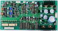 127A - Top of board, J-16 and optocouplers in bottom left
 -
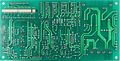 127A - Bottom of board, cutout under optocouplers in top left for high voltage isolation
 -
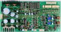 127B - Top of board, J-16 and optocouplers in top right
 -
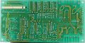 127B - Bottom of board, cutout under optocouplers in top left for high voltage isolation


Connector Map
| Connector | Direction | Function |
|---|---|---|
| J-12 | In | Three transformer secondaries plus a ground-tie wire — feeds the on-board rectifiers and ±15 V / +12 V / +5 V regulators (see J-12 Power-Input Topology below) |
| J-13 | In/Out | HV module interface (signal/feedback, near IR3M02 #1) |
| J-14 | In | Feedback from HV module output stage |
| J-15 | In/Out | Protection circuit (short / overcurrent / arc detection) |
| J-16 | In/Out | Ribbon to embedded controller — serial DAC code in, telemetry and status out via optocouplers |
J-12 Power-Input Topology

J-12 carries three transformer secondary windings plus a single ground-tie wire. The transformer itself has no center tap or earthed reference — the system ground is established on the board by bonding the negative DC output of one rectifier to the positive DC output of another, using the lone green wire. This stacks two of the rectified supplies end-to-end to produce the bipolar ±Vunreg rails feeding the ±15 V analog regulators, while the third (blue) winding feeds an independent positive rail for the digital regulators.
Stacked Topology
        +Vunreg  ──▶  μA 78M15  ──▶  +15 V analog
            ▲
   ┌────────┴────────┐
   │ Yellow pair     │ ← secondary winding #1
   │ → bridge rect.  │
   └────────┬────────┘
            │ "−" output of yellow rectifier
            ●━━━━━━━━━━━●  ◀── GREEN wire (system ground, 0 V)
            │ "+" output of red rectifier
   ┌────────┴────────┐
   │ Red pair        │ ← secondary winding #2
   │ → bridge rect.  │
   └────────┬────────┘
            ▼
        −Vunreg  ──▶  μA79M15A ──▶  −15 V analog


   ┌─────────────────┐
   │ Blue pair       │ ← secondary winding #3 (independent)
   │ → bridge rect.  │
   └────────┬────────┘
            ▼
        +Vunreg(logic) ──┬──▶ LM340T-12 ──▶ +12 V
                         └──▶ μA 78M05  ──▶  +5 V digital
Wire Color Map
| Wire | Conductors | Function | Feeds |
|---|---|---|---|
| Yellow | pair | Secondary winding #1, feeds bridge rectifier whose "+" output becomes +Vunreg | +15 V regulator (REG2) |
| Red | pair | Secondary winding #2, feeds bridge rectifier whose "−" output becomes −Vunreg | −15 V regulator (REG1) |
| Green | single | Ground bond — ties "−" of the yellow rectifier to "+" of the red rectifier, establishing the 0 V system reference | Analog ground for the entire board |
| Blue | pair | Secondary winding #3 (independent), feeds bridge rectifier for the positive logic rail | +12 V (REG3) and +5 V (REG4) regulators |
Notes on the Topology
- The transformer has three independent floating secondaries — no center tap is brought out. The bipolar ±15 V rail pair is synthesized on the board by stacking two single-ended supplies via the green ground-tie wire.
- The green wire is a current-carrying ground return, not just a reference. The imbalance current between the +15 V and −15 V loads flows through it back to the rectifier diodes, so it should be a reasonable gauge and routed for low loop inductance. Lifting it during service work will collapse the entire analog ground reference of the board.
- Because the "+" pin of the red bridge rectifier is bonded to ground, the red supply's negative DC output is the rail that goes down to the −15 V regulator. This is normal for a stacked topology but can be confusing if you expect the rectifier "+" pin to be the rail output.
- Keeping the digital +5 V / +12 V supply on its own winding (blue) isolates digital switching noise from the ±15 V analog rails, which carry the precision references for the AD7543 DAC and the AD654 V/F converters.
J-16 Data, Status and Telemetry

J-16 carries four data lines to an on-board AD7543 Digital to Analog Converter (DAC) which selects the voltage generated by the power supply. 0 - 4095 is the valid range to set ~20V to 3000V in 0.7V increments. It also has PWM outputs for voltage and current to monitor actual values and three additional I/O lines to signal Circuit Open, Circuit Shorted and one Circuit Unknown, possibly to signal a ground fault condition per the user manual. This connector goes straight to optocouplers so the control side is isolated from the high voltage side.
Pin Definitions
| Position | Function | Direction | To IC pin | Notes |
|---|---|---|---|---|
| 1 | +5V | Input | PC1-1,3,5,7 | Supplied by the logic board to the Optocoupler drivers used to send data to the DAC |
| 2 | Voltage PWM | Output | PC2-16 | PWM output corresponding to voltage level |
| 3 | Current PWM | Output | PC2-14 | PWM output corresponding to current draw |
| 4 | Circuit Unknown | Output | PC3-4 | Possibly a ground fault indicator |
| 5 | Circuit Open | Output | PC2-12 | Indicates if a load is connected to the High Voltage output |
| 6 | Circuit Shorted | Output | PC2-10 | Indicates if the High Voltage output is shorted |
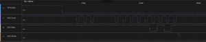
| 7 | HV Enable | Input | PC1-8 | Active Low - Set low to enable HV output control by DAC, set high to disable HV supply |
| 8 | DAC Clock | Input | PC1-6 | Active Low - 12 clock cycles |
| 9 | DAC Data | Input | PC1-4 | Active Low - Data MSB |
| 10 | DAC Strobe | Input | PC1-2 | Active High - Strobe signal at the end of the data load |
| 11, 12 | GND | Input | PC3-3
PC2-9,11,13,15 |
Ground supplied by logic board to Optocoupler receivers used to communicate back to logic board |
Timing Information
-
-
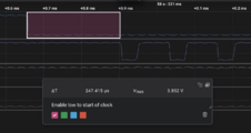 HV Enable low to start of data
 -
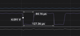 Clock signal timing
 -
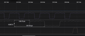 Data signal timing, centered within clock
 -
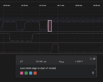 End of clock to strobe timing


Active Components
Switching-Regulator Controllers
| Part Number | Marking | Package | Function | Datasheet |
|---|---|---|---|---|
| Sharp IR3M02 (×2) | "SHARP IR3M02 78XD / 78SD" | 16-DIP | PWM switching-regulator control IC; upgraded IR9494 with under-voltage lockout. The two devices most likely implement the constant-voltage loop and constant-current loop independently — the active loop dominates per Bio-Rad's CV / CC / CP mode behavior. | PDF · datasheetcatalog |
Digital-to-Analog Converter
| Part Number | Marking | Package | Function | Datasheet |
|---|---|---|---|---|
| Analog Devices AD7543JN | "AD7543JN" | 16-DIP | CMOS 12-bit serial-input monolithic multiplying DAC, R-2R ladder. Has an internal 12-bit serial-in parallel-out shift register (Register A) plus a separate 12-bit DAC input register (Register B), so the chip accepts serial setpoint data directly from the μC — no external shift register required. The two-register architecture lets the μC clock in a new code while the DAC continues to hold the previous value, then transfer it cleanly with a LOAD pulse. Asynchronous CLEAR input zeroes Register B for safe initialization. With 12-bit resolution this gives ~0.7 V resolution at 3000 V full-scale — consistent with Bio-Rad's published 1 V step granularity. The "multiplying" feature is convenient because VREF can be scaled by an external precision reference for absolute-voltage trim. | AD7543 product page · PDF |
CMOS Logic (Toshiba 4000-series)
| Part Number | Marking | Package | Function | Datasheet |
|---|---|---|---|---|
| TC4011BP | "TOSHIBA 8838B TC4011BP JAPAN" | 14-DIP | Quad 2-input NAND gate. Likely used to combine fault / interlock / reset signals into the IR3M02 shutdown line and possibly to gate the AD7543 control inputs. | Toshiba page · PDF |
| TC4013BP | "TOSHIBA 8836HB TC4013BP JAPAN" | 14-DIP | Dual D-type flip-flop with set/reset. Strong candidate for the fault latch — set by a comparator output from J-15 (short / overcurrent / arc), output ties into the IR3M02 shutdown pin and stays latched until the μC issues an explicit reset. The second flip-flop may serve as a sync stage or as a divide-by-2 in an AD654 gate-timing chain. | Toshiba PDF |
| TC4025BP | "TOSHIBA 8844HB TC4025BP JAPAN" | 14-DIP | Triple 3-input NOR gate. Typical use in this kind of design: combining multiple shutdown sources (over-current, over-voltage, interlock-open, μC-stop) into a single active-high enable signal. | Toshiba PDF |
| TC4584BP | "TOSHIBA 8848H TC4584BP JAPAN" | 14-DIP | Hex Schmitt-trigger inverter. Confirmed to sit in the signal path between the input optocoupler bank and the AD7543, cleaning up the slow optocoupler-output edges and inverting them before they reach the DAC's clocked inputs (SRI / STB / LD / CLR), which require sharp transitions. With 6 cells available and 4 used for the DAC interface, up to 2 cells remain — likely used either for additional input cleanup (master enable, fault input from J-15) or configured as an RC oscillator providing a local time-base for AD654 gate timing. |
Operational Amplifiers (National Semiconductor)
| Part Number | Marking | Package | Function | Datasheet |
|---|---|---|---|---|
| LF353N (multiple) | "LF ⊗ 353N M8818" | 8-DIP | Dual JFET-input op-amp, low input bias, used where high Z input is needed (V/F front-end, integrator stages, HV-divider buffer). | TI PDF |
| LM358N (probable) (multiple) | "LM ⊗ … M8836" | 8-DIP | General-purpose dual op-amp, used as comparator / signal-conditioning. Suffix not fully readable in photos. | TI PDF |
Voltage-to-Frequency Converter (Analog Devices)
| Part Number | Marking | Package | Function | Datasheet |
|---|---|---|---|---|
| AD654JN (×2) | "AD654JN M8824A" | 8-DIP | Low-cost monolithic V/F converter, 0–500 kHz, ±0.03 % linearity. One channel measures HV (output voltage), the other measures HC (output current) — both reported back to the μC as a frequency through the optocoupler isolation barrier. Frequency-domain telemetry sidesteps optocoupler CTR drift. | AD PDF · AD page |
Optocouplers (Toshiba)
| Part Number | Marking | Package | Function | Datasheet |
|---|---|---|---|---|
| TLP621-4 (×2) | "T8K TLP621-4 GB" | 16-DIP | Quad transistor-output optocoupler, 5 kVrms isolation, CTR 100–600 %. Together they provide 8 isolated digital channels — sufficient for the AD7543's serial interface (SRI data, STB clock, LD load, CLR clear), master enable, fault status, plus the two AD654 frequency-out telemetry channels. | Datasheet |
| TLP621 (×1) | "T7K P621" | 4-DIP | Single-channel version. Probably an additional status / interlock line, or a high-priority signal kept on its own isolation domain. | Datasheet |
Linear Voltage Regulators (Confirmed from photos)
| Position | Part Number | Output | Datasheet |
|---|---|---|---|
| REG1 | 7805 | +5V Digital Rail | LM340 PDF (TI) |
| REG2 | 7815 | +15 V analog rail | 78xx PDF (TI) |
| REG3 | 7915 | −15 V analog rail | 79xx PDF (TI) |
| REG4 | 7812 | +12 V rail | 78M PDF (TI) |
Passive Components
| Type | Description |
|---|---|
| Trim pots (VR1–VR6) | Blue 25-turn cermet, Bourns 3296-style. Marking "78205" / "5028L" on the side is the manufacturer's part/style code, not the resistance. The resistance code is on the top face under the screw. Used for setting V/F scale & offset (per AD654 channel) and HV setpoint trims. Bourns 3296 datasheet |
| Large blue radial electrolytics | "CEW M97 / M404 85 °C" — Japanese-made (Nichicon or similar), main reservoir & rail filtering after the bridge rectifier. |
| Rubycon "25v 100μF" | Visible near REG3/REG4 — local rail decoupling. |
| Smaller blue electrolytics | Bypass and decoupling on each rail and around the IR3M02s. |
| Brown axial film cap (left edge) | Metalized polypropylene; safety / snubber. |
| Green disc ceramics | High-voltage Y-rated ceramic discs. |
| Two small bare-copper toroids (bottom) | Output filter inductors. |
| Large copper-wound toroid (top right) | Common-mode line-input choke. |
Reverse-Engineering Notes
- Two IR3M02 controllers fit Bio-Rad's published behavior of independent constant-voltage and constant-current regulation with automatic crossover. Whichever loop demands the lower duty cycle wins, which is the textbook way to implement CV/CC/CP modes. The pairing of trim pots VR1+VR2 / VR3+VR4 next to the two AD654s is consistent with calibrating two independent feedback channels (one for V, one for I).
- The AD7543 12-bit serial-input DAC confirms this is a fully digital setpoint architecture, not a potentiometer-driven supply. The controller clocks a 12-bit code into the DAC's internal Register A through one optocoupler channel (SRI) timed by another (STB), then issues a LOAD pulse on a third channel to transfer the new code to the DAC output (Register B). With 4096 codes across 3000 V full-scale, that's ~0.73 V LSB — Bio-Rad spec'd 1 V steps, which matches.
- Because the AD7543 has its own internal serial-in shift register, the TC4013 / TC4011 / TC4025 logic cluster is not performing serial-to-parallel conversion for the DAC. Instead, that logic most likely handles: (a) fault-latching (TC4013 D-flip-flop set by a comparator output from J-15, output ties into the IR3M02 shutdown pin until the μC issues a reset), (b) generating local timing or gate windows for the AD654 measurement cycle, and/or (c) combining manual-reset, interlock, and over-temperature signals into the master enable line.
- The AD654 + TLP621-4 telemetry path is the classical isolated-precision-measurement trick. Two channels — one for HV, one for HC — give the μC the data it needs to display "actual" values and run constant-power calculations. Frequency-domain transmission across the optocoupler sidesteps CTR drift and aging.
- TC4584 Schmitt is confirmed in the optocoupler-to-DAC path. Each of the four AD7543 control signals (SRI, STB, LD, CLR) passes through one Schmitt-inverter cell after the optocoupler before reaching the DAC. Note that the TC4584 cells are inverting — the logic polarity at the DAC pin is opposite the polarity at the optocoupler output, which matters when probing. Combined with the optocoupler's own inversion (the output transistor pulls low when the LED is on), the net polarity from μC to DAC is non-inverting.
- The J-12 power-input topology (three independent floating secondaries with on-board ground synthesis via the green ground-tie wire) means the entire OEM 127A board is referenced to its own analog ground, not chassis. Anything probing this board during operation must reference scope grounds to that node, not to chassis or earth, to avoid blowing up secondary windings or injecting ground loops.
Items Still to Confirm
- Resolve whether the +12 V regulator sits at REG3 or REG4 (silkscreen vs. position)
- Confirm "LM ⊗ M8836" parts are LM358N (vs LM833 etc.) under magnifier
- Verify all "M8818 LF" parts are LF353N (suffix not visible in all shots)
- Identify what J-13 carries (likely shares the HV-module signal bus with J-14)
- Probe the AD654 output frequencies at full-scale HV and full-scale HC to determine the monitoring scale factors
- Identify the two TO-220 transistors visible near the heatsinks at top-left of the board (driver pre-stage between IR3M02s and the HV switching FETs?)
- Trace the 9 optocoupler channels at J-16 (8 across the two TLP621-4 quads plus the 1 in the TLP621 single) and assign each a function. Expected set: AD7543 SRI / STB / LD / CLR (4), master ENABLE (1), FAULT status out (1), HV frequency out (1), HC frequency out (1), plus 1 reserved/interlock.
- Determine what role the TC4013 / TC4011 / TC4025 logic plays now that the DAC handles its own serial-to-parallel conversion (fault latch and/or AD654 gate-timing oscillator are the leading hypotheses).
OEM No. 126C
Module not yet examined. Photos and reverse-engineering pending.
OEM No. 128B
Module not yet examined. Photos and reverse-engineering pending.
OEM No. 130C
Module not yet examined. Photos and reverse-engineering pending.
OEM No. 131A
Module not yet examined. Photos and reverse-engineering pending.
Auxiliary Power Supply Module
Switch-mode housekeeping supply visible at the right side of the chassis. Not yet examined in detail.
Mains Transformer
Multi-secondary line-frequency transformer visible at the top-left of the chassis. Has at least three independent floating secondary windings brought out to the OEM No. 127A controller board via J-12:
- Yellow pair — secondary winding #1, feeds the +15 V analog rail
- Red pair — secondary winding #2, feeds the −15 V analog rail
- Blue pair — secondary winding #3, feeds the +12 V and +5 V digital rails
A single green wire also exits the harness at J-12 to bond the rectifier outputs into a stacked bipolar topology (see J-12 Power-Input Topology).
Voltage taps and current ratings TBD. Additional secondaries (if any) feeding the HV generation module are routed separately and have not yet been documented.
High Voltage Generation Module
Multi-PCB high-voltage assembly. Comprises the HV switching power stage, step-up transformer, and a Cockcroft–Walton or similar diode/capacitor multiplier producing the 0–3000 V output. Driven by J-14 from the OEM No. 127A controller; returns voltage and current sense signals via J-13 (and possibly J-14).
References
- Bio-Rad 3000Xi product information — historical Bio-Rad documentation (now superseded by the PowerPac HV family).
- Spectralab Scientific — 3000Xi listing
- Artisan Technology Group — 3000Xi page
This article documents an ongoing teardown. Identifications are best-effort from photographs of date-coded components (1987–1988). Please verify physically before relying on any information here for repair or redesign.