DFM-17 Radiosonde: Difference between revisions
Add part revision per https://siliconlabs.force.com/community/s/article/using-part-info-command-to-identify-ezradio-pro-part-number?language=en_US |
Add info from gx1400's data_dfm_RE repo, clean up formatting, add new graphics and new repo for T/H measurement |
||
| (4 intermediate revisions by 2 users not shown) | |||
| Line 16: | Line 16: | ||
*Bandwidth: ~10 kHz (Website lists <12) | *Bandwidth: ~10 kHz (Website lists <12) | ||
*Frequency range: 400 - 405.99 MHz | *Frequency range: 400 - 405.99 MHz | ||
*Modulation: GFSK | *Modulation: GFSK @ 1250 bits/s | ||
*TX Power: ~100mW | *TX Power: ~100mW | ||
*Error Correction: Code-spreading, interleaving | *Error Correction: Code-spreading, interleaving | ||
| Line 22: | Line 22: | ||
*GPS: U-Blox MAX-M8C-0-10 | *GPS: U-Blox MAX-M8C-0-10 | ||
*Transmitter: Si4063 | *Transmitter: Si4063 | ||
*Optional: | |||
**XDATA interface (24 bytes/s) | |||
**NFC ground check | |||
**Barometric pressure sensor. | |||
==Peripheral attachment points== | ==Peripheral attachment points== | ||
| Line 32: | Line 36: | ||
*LED_R = PB12 | *LED_R = PB12 | ||
====uBlox GPS (USART_2)==== | ====uBlox GPS (USART_2) - U11==== | ||
*PA3(RX) = GPS TXD (Pin 2) | *PA3(RX) = GPS TXD (Pin 2) | ||
*PA2(TX) = GPS RXD (Pin 3) | *PA2(TX) = GPS RXD (Pin 3) | ||
*PB8 = GPS 1pps (Pin 4) (LED next to flex cable connector) | *PB8 = GPS 1pps (Pin 4) (LED next to flex cable connector) | ||
*PC14 = RESET | |||
====UART via USB Port (USART_1)==== | ====UART via USB Port (USART_1)==== | ||
| Line 42: | Line 47: | ||
*PA9(TX) = USB D+ | *PA9(TX) = USB D+ | ||
*PA10(RX) = USB D- | *PA10(RX) = USB D- | ||
*PC2 = GND/VBus Pin? | |||
====Si4063 (SPI_1)==== | ====Si4063 (SPI_1) - U10==== | ||
*PB2 = CS/nSEL (Pin 15) | *PB2 = CS/nSEL (Pin 15) | ||
| Line 50: | Line 56: | ||
*PA6 = SDO (Pin 13) | *PA6 = SDO (Pin 13) | ||
*PA5 = SCLK (Pin 12) | *PA5 = SCLK (Pin 12) | ||
*PD0 = GPIO2 (Pin 19) | |||
*PA4 = GPIO3 (Pin 20) | |||
====XDATA Header (2x2 pin unpopulated)==== | |||
* | *PB11 = Pin 3 | ||
* | *PB10 = Pin 2 | ||
**Pads need solder bridge or 0 ohm links. Pin 1 or 4 can be bridged to act as GND. I suspect the SOT23-6 footprint is populated when xdata is in use. Unknown where the xdata perhipheral would get VCC. | |||
<gallery> | |||
File:Xdata_pinout_dfm17.jpg|alt=xdata interface pinout|XDATA interface pinout, numbered for clarity. Not official. | |||
</gallery> | |||
==IC Attachment Points== | |||
===STG719 (DPST) - U2=== | |||
*PC11 = IN (Pin 1) | *PC11 = IN (Pin 1) | ||
===STG719 (DPST) - U3=== | |||
*PD2 = IN (Pin 1) | *PD2 = IN (Pin 1) | ||
===STG719 (DPST) - U4=== | |||
*PB5 = IN (Pin 1) | *PB5 = IN (Pin 1) | ||
===STG719 (DPST) - U5=== | |||
*PB4= IN (Pin 1) | *PB4= IN (Pin 1) | ||
===DG636 (Dual DPST) - U6=== | |||
*VDD = ENABLE (always HIGH) (Pin 2) | *VDD = ENABLE (always HIGH) (Pin 2) | ||
* | *PA11, PB0, PA1 = A0 (Pin 1) | ||
* | *PC10 = A1 (Pin 14) | ||
===STG719 (DPST) - U7=== | |||
* | *PC10 (routes under STM) = IN (Pin 1) | ||
===SN74LV4053 (Triple 2Ch Mux/Demux) - U8=== | |||
*PB13 & PB14 = A (Pin 11) | *PB13 & PB14 = A (Pin 11) | ||
**STM pins connected by trace? ''Why? Read back?'' | **STM pins connected by trace? ''Why? Read back?'' | ||
* | *PC10 = B (Pin 10) & C (Pin 9) | ||
**IC pins connected by trace | **IC pins connected by trace | ||
===LMV761 (Comparator) - U9=== | |||
*PA12 & PB15 = OUT (Pin 4 via cap) | |||
===Analog Inputs to STM32=== | |||
*PA0 - Vbatt/Power supply voltage (needs confirmation, V measured at pin is VCC) | |||
*PB1 - Vbatt/Power supply current monitor (needs confirmation, V measured at pin seems to match 1V = 1A) | |||
===Battery Management IC=== | |||
*PC0 - Hold high to prevent BMS from removing battery power after boot up | |||
* | ===NFC/RFID 4k EEPROM - U12=== | ||
* | |||
*PC13 = RF WIP/Busy (Pin 7) | |||
*PB6 = SCL (Pin 6) | |||
*PB7 = SDA (Pin 5) | |||
*PC0 connected to Pin 1 (Vout) | |||
** NFC antenna pads are below left side 3 pins of uBlox module | |||
<br /> | <br /> | ||
| Line 188: | Line 217: | ||
|4BEB 8150 | |4BEB 8150 | ||
|[https://www.st.com/resource/en/datasheet/m24lr04e-r.pdf STMicroelectronics] | |[https://www.st.com/resource/en/datasheet/m24lr04e-r.pdf STMicroelectronics] | ||
|'' | |''Stores configuration of serial ports, sonde serial(?), calibration, and measurement sequences'' | ||
|- | |- | ||
|U13 | |U13 | ||
| Line 218: | Line 247: | ||
|- | |- | ||
|U16 | |U16 | ||
| | |??? | ||
| | |??? | ||
| | |??? | ||
| | |??? | ||
|AL | |AL | ||
___ | |||
| | | | ||
|''In-line with battery power, need more information; chip marking'' | |''In-line with battery power, need more information; chip marking'' | ||
|- | |- | ||
|U17 | |U17 | ||
| | |??? | ||
| | |??? | ||
| | |??? | ||
| | |??? | ||
| | |??? | ||
| | |??? | ||
|''Connected to USB data lines, likely a UART, isolation, and/or level shifter'' | |''Connected to USB data lines, likely a UART, isolation, and/or level shifter'' | ||
|} | |} | ||
* Do note these reference designators are not official and are here for us to keep track. The PCB has no markings. | |||
<br /> | <br /> | ||
==Photos== | ==Photos== | ||
<gallery> | <gallery> | ||
| Line 249: | Line 278: | ||
File:V719 and others removed.jpg|V719 SOT-23-6 packages removed as well as 636EE (SPDT Switch) and LW053A (Mux/Demuxer) | File:V719 and others removed.jpg|V719 SOT-23-6 packages removed as well as 636EE (SPDT Switch) and LW053A (Mux/Demuxer) | ||
File:Stalk pinout mapping.png|Mapping of the pins on the sensor stalk to the connector and their corresponding IC/IO lines. '''''<u>Top of sensor stalk corresponds to bottom of pictured connector!</u>''''' | File:Stalk pinout mapping.png|Mapping of the pins on the sensor stalk to the connector and their corresponding IC/IO lines. '''''<u>Top of sensor stalk corresponds to bottom of pictured connector!</u>''''' | ||
File: | File:Dfm17_barepcb_back_traces.jpg|Bare PCB without major ICs on it and rear traces colored in purple. Any other via goes directly to main groundplane. | ||
</gallery> | </gallery> | ||
==Disassembly== | ==Disassembly== | ||
| Line 282: | Line 312: | ||
*VBUS: 5 Volts DC | *VBUS: 5 Volts DC | ||
*D-: TX | *D- (typically white): TX | ||
*D+: RX | *D+ (typically green): RX | ||
*GND: GND | *GND: GND | ||
| Line 291: | Line 321: | ||
==Hardware modifications== | ==Hardware modifications== | ||
====SMA Port | ====SMA Port==== | ||
The | The DFM17 antenna section has pads sized for an SMA connector (likely leftover from development). Any board edge mount conector should work. | ||
====SWD Header==== | |||
To program the DFM, you will need to connect to the SWD header. If you want to do it properly, an [https://adafru.it/4048 Adafruit Skinny SWD SMT] connector will fit. You can also 3D print [https://www.printables.com/model/594752-dfm17-swd-programming-jig-clip-thing this model] by trickv to clamp the connector to the pads for a solderless approach. | |||
I suggest also ordering [https://www.adafruit.com/product/1675 this ribbon cable] and [https://www.adafruit.com/product/2743 this breakout] to be able to attach to your STLink much easier. | |||
Do note that if you wish to put the PCB back in the styrofoam housing, you will need to slice away some of the inside to allow the connector to fit. Approximately 40mm or so. You will need to do this if you attach pin headers for xdata as well. | |||
====Minimizing transmit range | ====Minimizing transmit range==== | ||
As amateurs we are not licensed to transmit in the 400-406MHz band, so for testing purposes one should perform this mod. | As amateurs we are not licensed to transmit in the 400-406MHz band, so for testing purposes one should perform this mod. If you have an appropriate SMA connector, solder it in place of the antenna wire and connect a 50 ohm dummy load to it (reminder that the power is approx 100mW). | ||
If no connector is available, unsolder the antenna wire and take two 100 ohm resistors and twist them in parallel, then solder them to the center pad and one of the side pads on the SMA footprint. This creates a 50 ohm dummy load for the Si4036 to transmit into. The range is reduced to a couple tens of feet. | |||
<u>'''Also if you are running a radiosonde_auto_rx instance, don't forget to turn it off during testing to avoid feeding erroneous data to Sondehub!'''</u> | |||
<gallery> | |||
File:Modified DFM-17 Radiosonde.jpg|MrARM's modified DFM-17 with a SWD connector and an SMA antenna port | File:Modified DFM-17 Radiosonde.jpg|MrARM's modified DFM-17 with a SWD connector and an SMA antenna port | ||
File:Dfm 17 swd and resistors.jpg|Trevor229's DFM with ST-Link SWD pins connected to debug interface and 50 ohm dummy load mod. | File:Dfm 17 swd and resistors.jpg|Trevor229's DFM with ST-Link SWD pins connected to debug interface and 50 ohm dummy load mod. | ||
</gallery> | </gallery> | ||
==Developing and Programming the board== | ==Developing for and Programming the board== | ||
[[File: | [[File:Dfm17_swd_pinout_pretty.jpg|thumb|Pinout of the SWD Port]] | ||
When lab testing, you can power the board from the USB header. It also appears to run fine supplying 3.3V to the SWD port (STLink and clones do this). | |||
The board uses a STM32, and requires a ST-Link to program. The process used to upload code to the MCU is the same as the Vaisala RS41 radiosonde, you will need to connect the VTRef(3.3V), Ground, SWDIO, SWDCLK and RST pins to your ST-Link. | |||
The board can run without external power being supplied when programming. This board has read-out protection enabled similar to the RS41 and this must be disabled before you can flash firmware to the board. | |||
==Software== | |||
A few attempts have been made to build replacement firmware for these devices, the key goal being to be able to re-fly a sonde as an amateur payload. | |||
There was an early attempt called dfm17_hamradio [https://github.com/gx1400/dfm17_hamradio here] and [https://github.com/trickv/dfm17_hamradio/tree/aprs-fifo-gps-superhacky here]. | |||
The most mature looking effort is [https://github.com/mikaelnousiainen/RS41ng RS41ng] which has experimental support. | |||
There is now a repository that uses code from RS41ng to run the sampling circuitry and read from the original temperature and humidity sensors [https://github.com/robots/radiosonde_dfm17 here.] | |||
<references /> | <references /> | ||
Latest revision as of 22:48, 24 January 2025
The DFM-17 is a balloon-launched radiosonde manufactured by GRAW Radiosondes GmbH & Co. KG, and used for meteorological sounding.

Overview
The DFM-17 radiosonde succeeds the DFM-09 radiosonde. Graw began a contract with NOAA in the US to provide radiosondes. As of Late 2021, several sites have made the transition as part of NOAA’s Operational Test and Evaluation (OT&E) program. 45 CONUS sites are expected to use these radiosondes in early 2022. [1]
Specs [2]
- Weight: 63g
- Size: 90 x 67 x 44 mm
- Power supply: 2 CR123A batteries
- Estimated runtime: ~240 minutes
- Transmission rate: 1 packet/sec
- Bandwidth: ~10 kHz (Website lists <12)
- Frequency range: 400 - 405.99 MHz
- Modulation: GFSK @ 1250 bits/s
- TX Power: ~100mW
- Error Correction: Code-spreading, interleaving
- SoC: STM32F100R8T6B, 24MHz, 8KB RAM, 64KB Flash
- GPS: U-Blox MAX-M8C-0-10
- Transmitter: Si4063
- Optional:
- XDATA interface (24 bytes/s)
- NFC ground check
- Barometric pressure sensor.
Peripheral attachment points
LED's and Buttons
- Button = PC8
- LED_Y = PC7
- LED_G = PC6
- LED_R = PB12
uBlox GPS (USART_2) - U11
- PA3(RX) = GPS TXD (Pin 2)
- PA2(TX) = GPS RXD (Pin 3)
- PB8 = GPS 1pps (Pin 4) (LED next to flex cable connector)
- PC14 = RESET
UART via USB Port (USART_1)
- PA9(TX) = USB D+
- PA10(RX) = USB D-
- PC2 = GND/VBus Pin?
Si4063 (SPI_1) - U10
- PB2 = CS/nSEL (Pin 15)
- PC3 - SDN (Pin 1)
- PA7 = SDI (Pin 14)
- PA6 = SDO (Pin 13)
- PA5 = SCLK (Pin 12)
- PD0 = GPIO2 (Pin 19)
- PA4 = GPIO3 (Pin 20)
XDATA Header (2x2 pin unpopulated)
- PB11 = Pin 3
- PB10 = Pin 2
- Pads need solder bridge or 0 ohm links. Pin 1 or 4 can be bridged to act as GND. I suspect the SOT23-6 footprint is populated when xdata is in use. Unknown where the xdata perhipheral would get VCC.
-
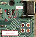 XDATA interface pinout, numbered for clarity. Not official.

IC Attachment Points
STG719 (DPST) - U2
- PC11 = IN (Pin 1)
STG719 (DPST) - U3
- PD2 = IN (Pin 1)
STG719 (DPST) - U4
- PB5 = IN (Pin 1)
STG719 (DPST) - U5
- PB4= IN (Pin 1)
DG636 (Dual DPST) - U6
- VDD = ENABLE (always HIGH) (Pin 2)
- PA11, PB0, PA1 = A0 (Pin 1)
- PC10 = A1 (Pin 14)
STG719 (DPST) - U7
- PC10 (routes under STM) = IN (Pin 1)
SN74LV4053 (Triple 2Ch Mux/Demux) - U8
- PB13 & PB14 = A (Pin 11)
- STM pins connected by trace? Why? Read back?
- PC10 = B (Pin 10) & C (Pin 9)
- IC pins connected by trace
LMV761 (Comparator) - U9
- PA12 & PB15 = OUT (Pin 4 via cap)
Analog Inputs to STM32
- PA0 - Vbatt/Power supply voltage (needs confirmation, V measured at pin is VCC)
- PB1 - Vbatt/Power supply current monitor (needs confirmation, V measured at pin seems to match 1V = 1A)
Battery Management IC
- PC0 - Hold high to prevent BMS from removing battery power after boot up
NFC/RFID 4k EEPROM - U12
- PC13 = RF WIP/Busy (Pin 7)
- PB6 = SCL (Pin 6)
- PB7 = SDA (Pin 5)
- PC0 connected to Pin 1 (Vout)
- NFC antenna pads are below left side 3 pins of uBlox module
Identified Supplementary IC's
-
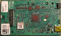 Top view of PCB with U reference designators overlaid

| Manufacturer | Part Number | Description | Package | Part Marking | Datasheet | Note | |
|---|---|---|---|---|---|---|---|
| U1 | STMicroelectronics | STM32F100R8T6B | ARM MCU, 24MHz, 8KB RAM, 64KB Flash | LQFP48 | ARM 32F100R8T6B | Mouser | Some recent batches of the DFM-17 have been using knockoff STM32s! The chip shortage strikes again! |
| U2, U3, U4, U5, U7 | ST | STG719 | STG719STR Low Voltage 4 Ohm SPDT Switch | SOT-23-6 | V719 | Mouser | Analog ADG719 pin compatible equivalent? |
| U6 | Vishay | DG636E | 0.3 pC Charge Injection, 100 pA Leakage
CMOS ± 5 V / 5 V / 3 V Dual SPDT Analog Switch |
TSSOP14 | 636EE | Mouser | |
| U8 | Texas Instruments | SN74LV4053A | Triple 2-Channel Analog Multiplexer/Demultiplexer | SOT-23-6 | LW053A | Texas Instruments | |
| U9 | Texas Instruments | LMV761 | Low Voltage Precision Comparator with Push/Pull Output | SOT-23-6 | C22A | Texas Instruments | |
| U10 | Silicon Labs | Si4063-C2A | High Performance, Low Current Transmitter | QFN20 | 40632A
C01Q81 2217 |
Silcon Labs | |
| U11 | u-Blox | MAX-M8C-0-10 | u-blox M8 GNSS module, ROM, crystal | MAX-M8C-0-10 | u-Blox | ||
| U12 | STMicroelectronics | M24LR04E-R | Dynamic NFC/RFID tag IC with 4-Kbit EEPROM,
energy harvesting, I²C bus and ISO 15693 RF interface |
UDFN8 | 4BEB 8150 | STMicroelectronics | Stores configuration of serial ports, sonde serial(?), calibration, and measurement sequences |
| U13 | STMicroelectronics | LD series, unsure on specific part | 3.3V Low Drop Out Voltage Regulator | DFN6 | 33R | Possible part from Mouser | Needs verification, appears to provide 3.3V regulated power |
| U14 | Looks like a high side current monitor amplifier, need more information | ||||||
| U15 | ABLIC | S-8200A Series, unsure on specific Part Number | BATTERY PROTECTION IC FOR 1-CELL PACK | VDL | Mouser | Needs verification, Potentially a Winsok WSTDW01 Battery Protection IC? | |
| U16 | ??? | ??? | ??? | ??? | AL
___ |
In-line with battery power, need more information; chip marking | |
| U17 | ??? | ??? | ??? | ??? | ??? | ??? | Connected to USB data lines, likely a UART, isolation, and/or level shifter |
- Do note these reference designators are not official and are here for us to keep track. The PCB has no markings.
Photos
-
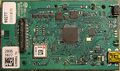 Internal view of the DFM-17
 -
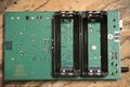 The bottom side of the PCB in the DFM-17
 -
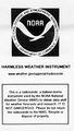 The label sticker NOAA(US) puts on the back of their DFM-17 radiosondes
 -
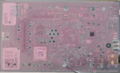 A view of the DFM-17 Radiosonde showing both layers to better assist tracing connections while reverse engineering the hardware.
 -
![Possible meanings of the internal labels and values. The date code in particular which may be useful to date production times. NWS sondes have the same cryptic string printed on the outside of the sonde where the mfg. date normally is on other countries'. "TU" may just indicate the board comes with sensors according to a third party source[3].](/w/images/thumb/7/7d/Label_id_speculaton.jpg/120px-Label_id_speculaton.jpg) Possible meanings of the internal labels and values. The date code in particular which may be useful to date production times. NWS sondes have the same cryptic string printed on the outside of the sonde where the mfg. date normally is on other countries'. "TU" may just indicate the board comes with sensors according to a third party source[3].
Possible meanings of the internal labels and values. The date code in particular which may be useful to date production times. NWS sondes have the same cryptic string printed on the outside of the sonde where the mfg. date normally is on other countries'. "TU" may just indicate the board comes with sensors according to a third party source[3]. -
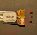 Pinout of the DFM-17 sensor stalk. Not all pins are used, and some seemingly are connected to a trace but end abruptly.
 -
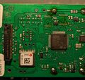 V719 SOT-23-6 packages removed as well as 636EE (SPDT Switch) and LW053A (Mux/Demuxer)
 -
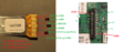 Mapping of the pins on the sensor stalk to the connector and their corresponding IC/IO lines. Top of sensor stalk corresponds to bottom of pictured connector!
 -
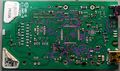 Bare PCB without major ICs on it and rear traces colored in purple. Any other via goes directly to main groundplane.


![Possible meanings of the internal labels and values. The date code in particular which may be useful to date production times. NWS sondes have the same cryptic string printed on the outside of the sonde where the mfg. date normally is on other countries'. "TU" may just indicate the board comes with sensors according to a third party source[3].](/view/File:Label_id_speculaton.jpg)


Disassembly
- Examine rope, parachute and parachute rigging lines for viability. Neatly organize the flight rigging if usable. Discard if not viable for reuse.
- Cut the zip tie surrounding the Styrofoam from the top portion by the rope loop.
- Pull the rope loop out, there should be little to no resistance.
- Make a slice in the sticker[4] where the two pieces of Styrofoam meet.
- Pull apart the two Styrofoam pieces to reveal the circuit board.
- Pull the circuit board out. There will be some resistance.
- The board is now separated from the Styrofoam shell, reuse if desired.
- Pull the two CR123A batteries out, keep or discard them. The board can run off USB power. Batteries are not necessary for development on this board.
Reassembly
- Insert two fresh CR123A batteries into the board.
- Line up the board to the IO cutouts in the Styrofoam, begin to push into the slots. Make sure the antenna wire comes through.
- Press the top piece of Styrofoam into place.
- Tape or apply another sticker onto the back label. (Optional)
- Insert the plastic rope loop piece.
- zip tie the shell together, the zip tie end should end up on the edge nearest to the power button.
- Rope on a balloon/drone/kite/etc.. to the rope loop.
- Power on the device by pressing and holding the button, you will see a yellow light blink, hold until the light turns solid.
Mini USB Port
The mini USB port on the board does not use the USB protocol for communication, it is a UART bus. However using USB to power the board should not harm the board in theory.
In order to use it, splice a USB cable and wire up a USB<->TTL adapter with the following pins:
- VBUS: 5 Volts DC
- D- (typically white): TX
- D+ (typically green): RX
- GND: GND
The board will communicate with the official GRAWMET software using this approach. Reverse engineering of the port's protocol is underway, however it is believed to use a similar, if not the same protocol the PS-15 uses.
Hardware modifications
SMA Port
The DFM17 antenna section has pads sized for an SMA connector (likely leftover from development). Any board edge mount conector should work.
SWD Header
To program the DFM, you will need to connect to the SWD header. If you want to do it properly, an Adafruit Skinny SWD SMT connector will fit. You can also 3D print this model by trickv to clamp the connector to the pads for a solderless approach.
I suggest also ordering this ribbon cable and this breakout to be able to attach to your STLink much easier.
Do note that if you wish to put the PCB back in the styrofoam housing, you will need to slice away some of the inside to allow the connector to fit. Approximately 40mm or so. You will need to do this if you attach pin headers for xdata as well.
Minimizing transmit range
As amateurs we are not licensed to transmit in the 400-406MHz band, so for testing purposes one should perform this mod. If you have an appropriate SMA connector, solder it in place of the antenna wire and connect a 50 ohm dummy load to it (reminder that the power is approx 100mW). If no connector is available, unsolder the antenna wire and take two 100 ohm resistors and twist them in parallel, then solder them to the center pad and one of the side pads on the SMA footprint. This creates a 50 ohm dummy load for the Si4036 to transmit into. The range is reduced to a couple tens of feet.
Also if you are running a radiosonde_auto_rx instance, don't forget to turn it off during testing to avoid feeding erroneous data to Sondehub!
-
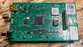 MrARM's modified DFM-17 with a SWD connector and an SMA antenna port
 -
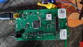 Trevor229's DFM with ST-Link SWD pins connected to debug interface and 50 ohm dummy load mod.


Developing for and Programming the board

When lab testing, you can power the board from the USB header. It also appears to run fine supplying 3.3V to the SWD port (STLink and clones do this).
The board uses a STM32, and requires a ST-Link to program. The process used to upload code to the MCU is the same as the Vaisala RS41 radiosonde, you will need to connect the VTRef(3.3V), Ground, SWDIO, SWDCLK and RST pins to your ST-Link.
The board can run without external power being supplied when programming. This board has read-out protection enabled similar to the RS41 and this must be disabled before you can flash firmware to the board.
Software
A few attempts have been made to build replacement firmware for these devices, the key goal being to be able to re-fly a sonde as an amateur payload.
There was an early attempt called dfm17_hamradio here and here.
The most mature looking effort is RS41ng which has experimental support.
There is now a repository that uses code from RS41ng to run the sampling circuitry and read from the original temperature and humidity sensors here.
- ↑ GRAW delivers to USA NOAA/National Weather Service. GRAW Radiosondes GmbH & Co. KG. Retrieved 17 November 2021.
- ↑ https://www.graw.de/products/radiosondes/dfm-17/
- ↑ https://sondehunt.de/language/en/archive/1189
- ↑ File:DFM-17 NOAA Label.jpg