Topping PA5
Contents
Topping PA5 Class-D Amplifier
The Topping PA5 Class-D Amplifier ist a small, affordable Stereo Amplifier consisting of a fully Balanced Pre and Post-Amp section with 2 Selectable Inputs via 6.35mm ( 1/8" ) Input jacks.
It is highly regarded in the HiFi Measurement community as it features a exceptionally low noisefloor and distortion [1].
Due to a major design flaw, a high failure rate has been reported [2], which led the Manufacturer to wipe its existence from its Website replacing it by the newer PA5 II which made changes in its layout to prevent or at least slow down the issue.
It is supplied by a 38V 5A Switchmode-Powersupply with a GX12 2pin Connector.
Board Layout
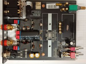
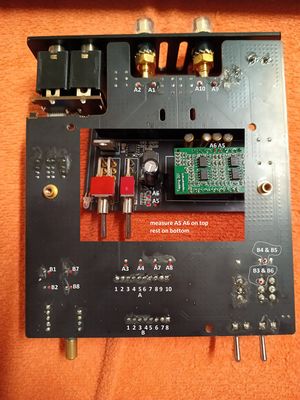
The Board consists of a 4 Layer PCB with its majority of Signal and Control lines routed on Top and Bottom.
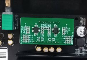
It features a soldered on Module labeled "Topping D01" which contains the Pre-amplifier section and the secret sauce to achieve these exceptional THD+N figures.
The Main amplifier chip is a Texas Instruments TPA3251 running at around 36VDC.
It gets its Gate Drive Supply GVDD Voltage of 12V from a TPS5430 DC-DC Converter
Its arrangement is a Differential Input BTL setup allowing for each Terminal to have its own Amplifier fed by a fully symmetrical input section decoupled by the golden Capacitors near the Chip and Volume-Control Pot.
There are two relais near the Input board to select either Input1 or Input2.
On the Power input section it features a soft-start and reverse polarity protection circuitry.
For supplying the Pre-amp module D01 (not populated in the Top Side Picture) a LM317 is used to generate 34.5V from the 38V Input supply, to filter out some of the Switchmode-Powersupply Noise.
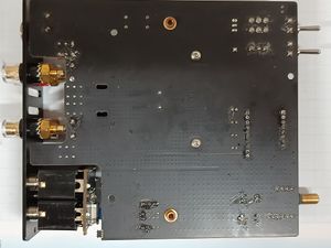
The Bottom part is empty to allow for cheaper assembly.
4 Traces coming from the Output jacks to the D01 module pins can be seen,
which indicate that their TPS supported Post-Filter Feedback feature is utilized.
Reverse-engineering attempts
A unusual high failure rate has been reported after the first few months of usage.
This led to investigating what went wrong and potentially finding a fix for this issue.
Amplifiers started to go crackle, pop, hiss and other unwanted effects on either one or both channels.
By tracing back the Signal path, i turned out to be the D01 Module that caused these issues.
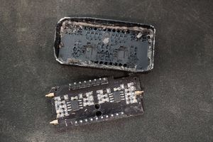
The module is covered by a metal lid that has "Topping D01" written on it which was potted in epoxy resin to prevent reverse-engineering attempts and protect their intellectual property.
It turned out, the potting compound expands and contracts with temperature changes, by packing in 4 Opamps enough heat was generated to cause issues.
By doing so, it stresses Solder joints and might crack them after many cycles.
Their attempt to keep people out only made them have a reason to get in, to fix their expensive little Amplifier.
The Compound was not intended for thermal equalization, this is still a Audio Amplifier, not a device to measure signals from the edge of space.
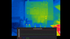
A thermal view of the new replacement module shows where heat is generated the most open air, within a encapsulated resin box it only could get worse.
To free it up, the module needed to be desoldered and heated by a Hot air station to around 350°C, at this stage the Potting compound became brittle and could be scraped and chipped off with a needle and tweezers.
The PCB consisted of dual-sided design, two stages of amplification and a PFFB filter network.
The components used were Texas Instruments OPA1612 Op-amps in the first-stage and NE5532 in the second-stage.
The OPA1612 have a very low noisefloor of only 5nV/√Hz at 1kHz and high Common-Mode Rejection ratio of 100dB typical, ideal for a low-noise input section.
The second stage consisting of two NE5532 is allready being fed from the first-stage amplified signal, so a higher noisefloor of the used opamps is neglible. It is just to add more gain and drive the output properly, as the NE5532 has higher output current capability.
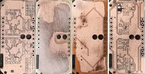
By sanding down the PCB it turned out to be 4 Layer with the Signal lines on Top and Bottom, VCC and GND in either inner Layer
The Metal lid ist just for Looks, it doesnt serve any other purpose like shielding.
The board has spring loaded pogo pins to keep it in place when potting it in the factory, but they are not connected to Ground. It is a floating piece of metal.
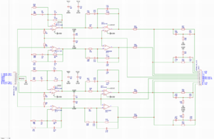
From these Layer Scans and the measured Components, a Schematic diagram was reverse-engineered.
This clearly shows the 4 Channel (Each side positive and negative) Low-noise input section utilizing the OPA1612 Opamps in a negative-feedback arrangement.
The second stage consisting of NE5532 is in a inverting configuration.
Due to the use of a Single supply, the Center points have been shifted to VCC/2 supplied by the pins marked (wrongly) as MUTE SW L and MUTE SW R which is generated near the Input selection switch as seen on the Top Side PCB view.
The signals coming out of C1 to C4 are going trough a decoupling capactor each into the TPA3251 Chip.
The FB lines are coming from the Speaker Terminals and are part of the PFFB circuitry, which all parts on the right side are dedicated to.
Topping used slightly different parts and values than the Official PFFB Guide suggested.
Replacement Module
Version 1
From all of this a new PCB could be created to replace the failed modules, as removing the Original PCB for repair was out of scope for most Users.
It was made using a 4 Layer PCB and populating both sides. This later turned out to be a major Cost to be avoided.
Version 2
In Version 2, a Single-sided only approach was taken to greatly reduce assembly costs.
It is still using a 4 layer PCB.
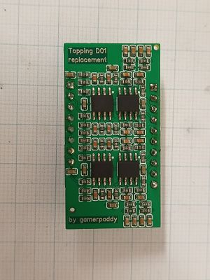
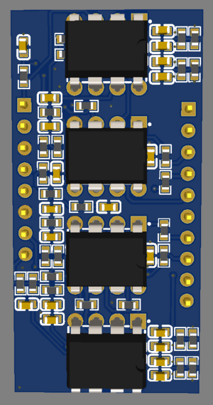
Version DIP
A common trend in the HiFi Community is Op-amp swapping to find the best sounding one.
This is highly debated as personal preferences are strongly influenced by other factors than just facts as in measurements.
This version features 4 DIP footprints on a single sided PCB, it contains components underneath the DIP parts to save space.
Version summary & Design files
All of the Versions can be found on the OSHW Project Page by opening the appropriate layout file in the Editor
Fix when a Repair goes wrong.
Due to the nature of being a multi-layered PCB with a big grounding plane and thin traces, heating the unleaded-solder properly to free up the old, broken Module, it can happen that Signal traces are ripped off the board.
Check each point to the counterpart for continuity and add jumpers accordingly if there is no continuity.
Changes in later versions of the PA5 Amplifier
In the PA5 II amplifier, Topping moved the Opamps out of the Potted modules to prevent them from being heated too much.
They are still in a not so well ventilated metal case and might fail someday too.
