Uploads by Trevor229
Jump to navigation
Jump to search
This special page shows all uploaded files.
| Date | Name | Thumbnail | Size | Description | Versions |
|---|---|---|---|---|---|
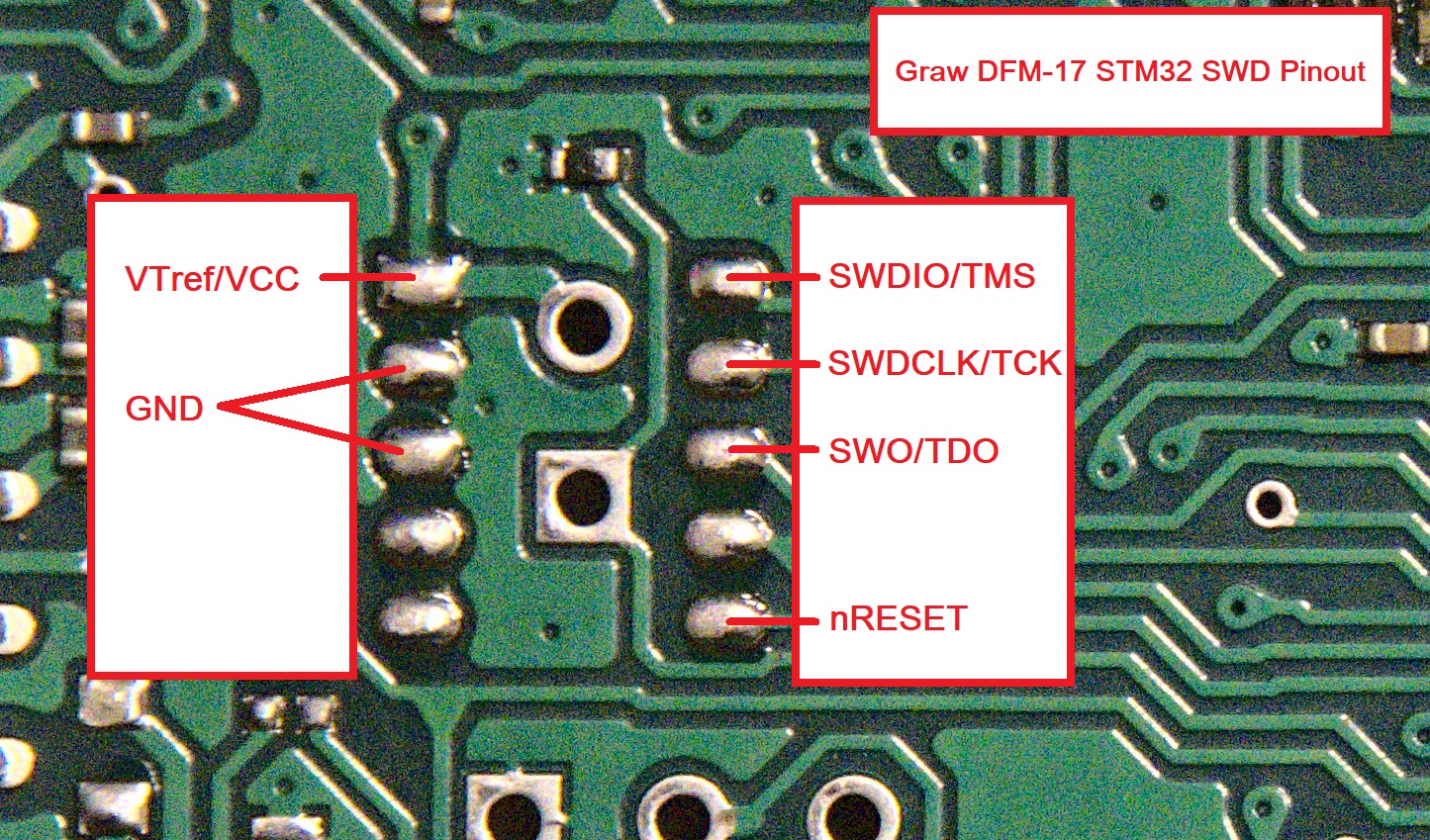
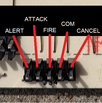
| 22:28, 24 January 2025 | Dfm17 swd pinout pretty.jpg (file) |  |
797 KB | 1 | |
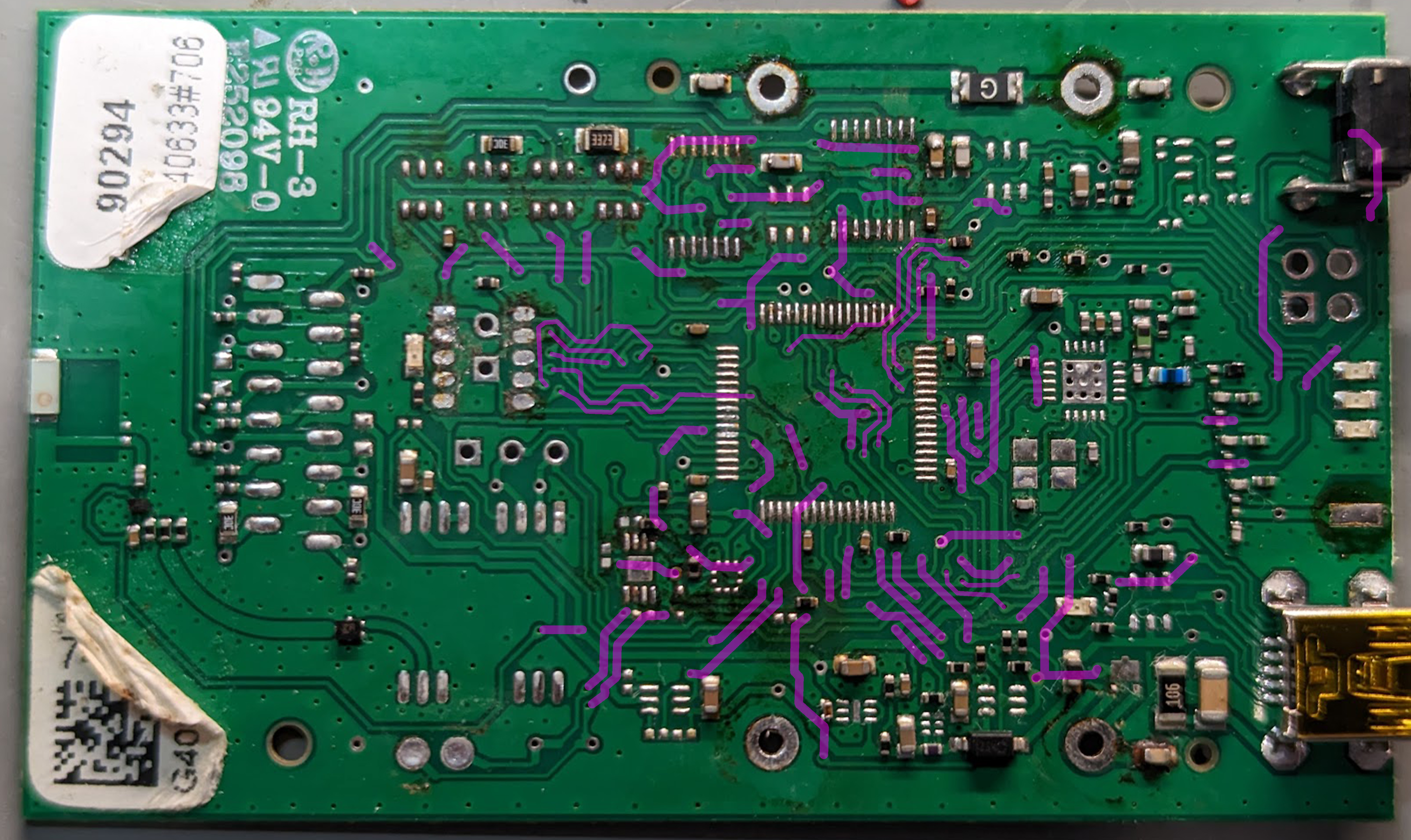
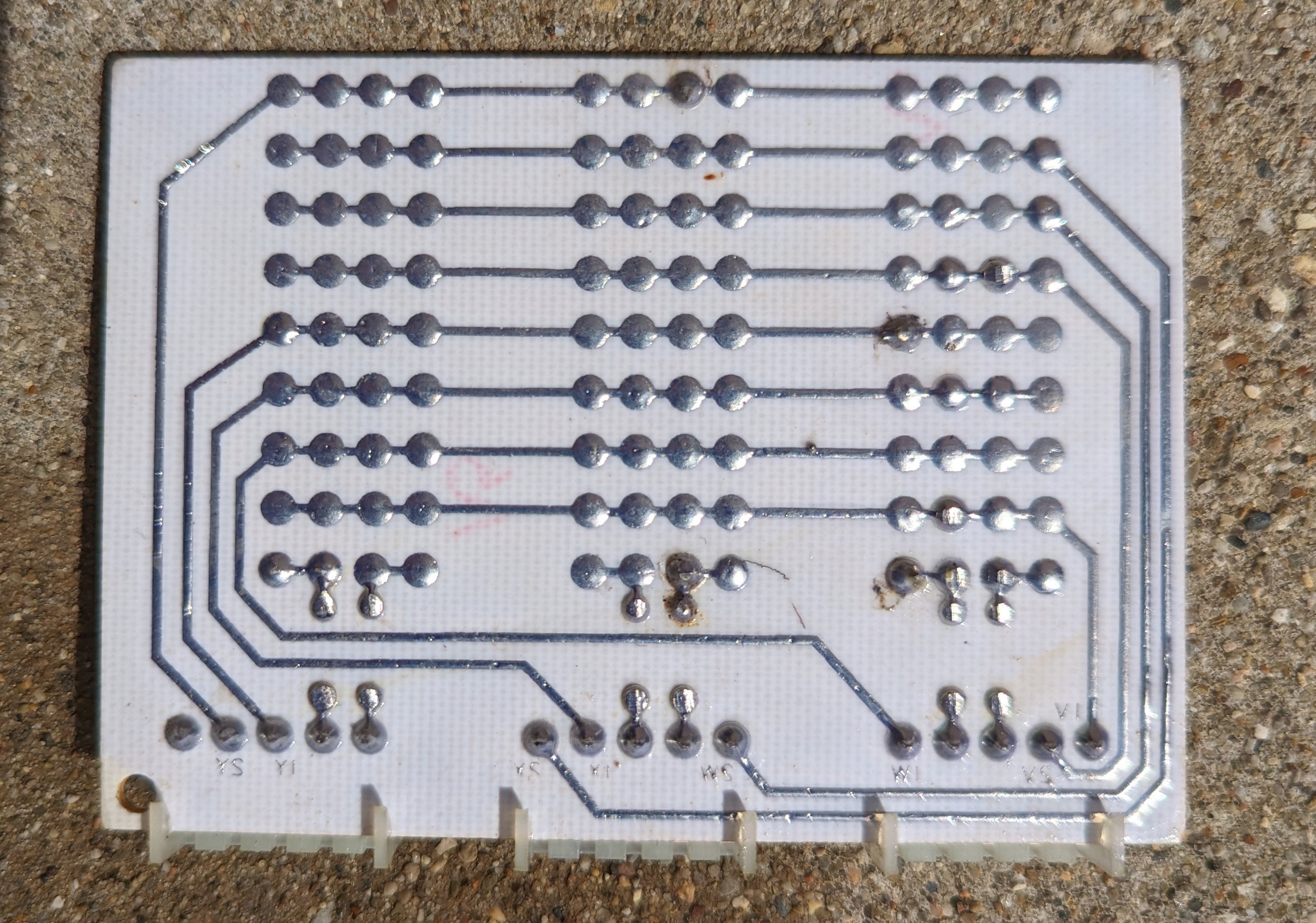
| 22:04, 24 January 2025 | Dfm17 barepcb back traces.jpg (file) |  |
2.67 MB | 1 | |
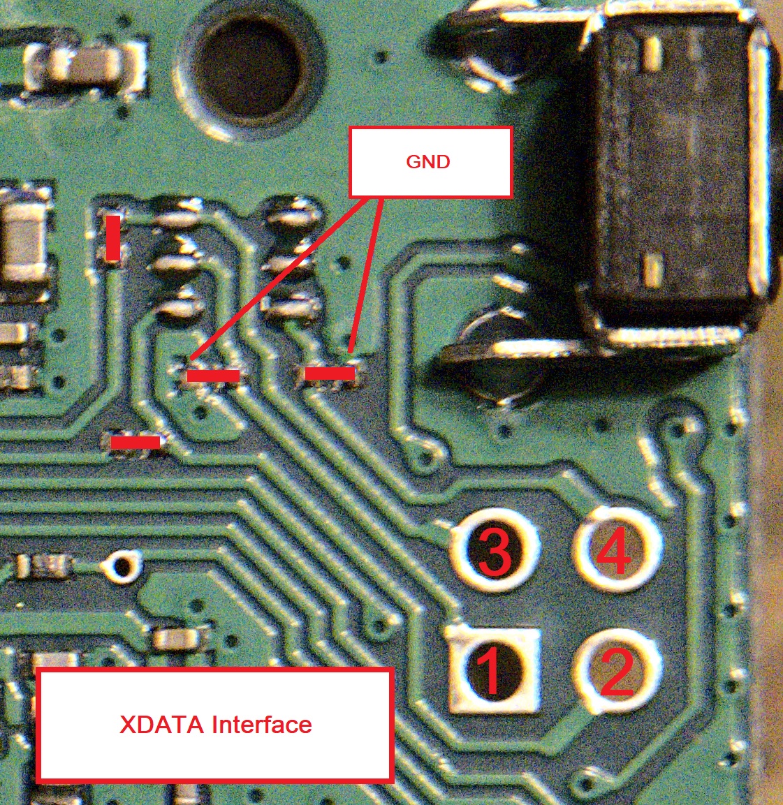
| 22:00, 24 January 2025 | Xdata pinout dfm17.jpg (file) |  |
822 KB | 1 | |
| 02:08, 17 August 2024 | Norcommnc401.pdf (file) | 3.33 MB | PDF user manual for the Norcomm NC401 DTMF decoder module | 1 | |
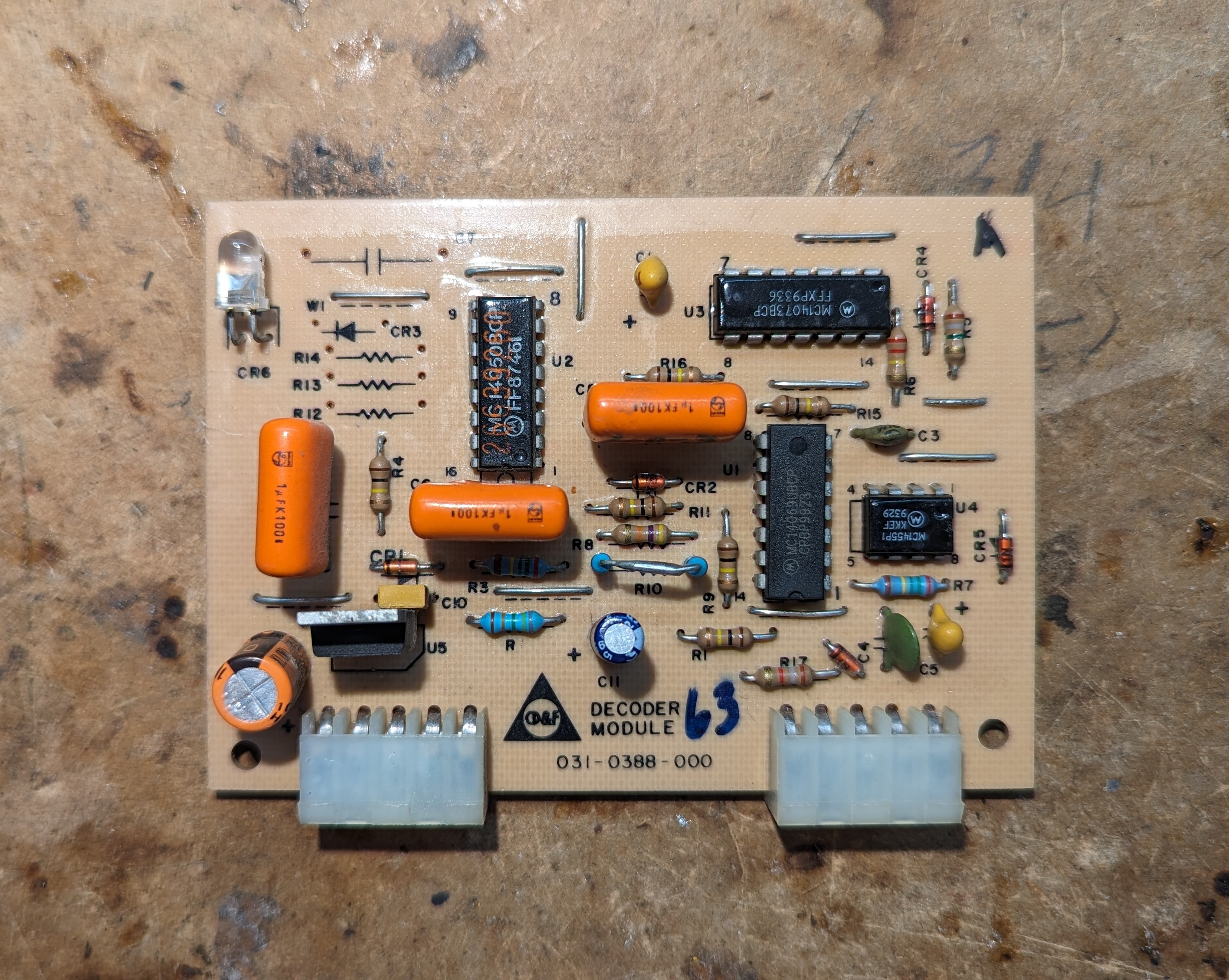
| 02:06, 17 August 2024 | Cdf decoder dtmf.jpg (file) |  |
1.26 MB | A DTMF version of a CD&F tone decoder module | 1 |
| 00:29, 25 May 2024 | Maxon sd blank configs.zip (file) | 1 KB | Blank configuration files for the Maxon SD-161/164 and SD-171/174 line of radios. | 1 | |
| 18:48, 23 May 2024 | Cdf SC hinge side.jpg (file) |  |
1.86 MB | Hinge side of the SC series CD&F | 1 |
| 18:48, 23 May 2024 | Cdf SC latch side.jpg (file) |  |
2.28 MB | Latch side of the SC series CD&F | 1 |
| 18:47, 23 May 2024 | Cdf SC back.jpg (file) |  |
1.39 MB | Back of the SC series CD&F | 1 |
| 18:47, 23 May 2024 | Cdf SC bottom.jpg (file) |  |
551 KB | Bottom of the SC series CD&F showing optional SO-239 | 1 |
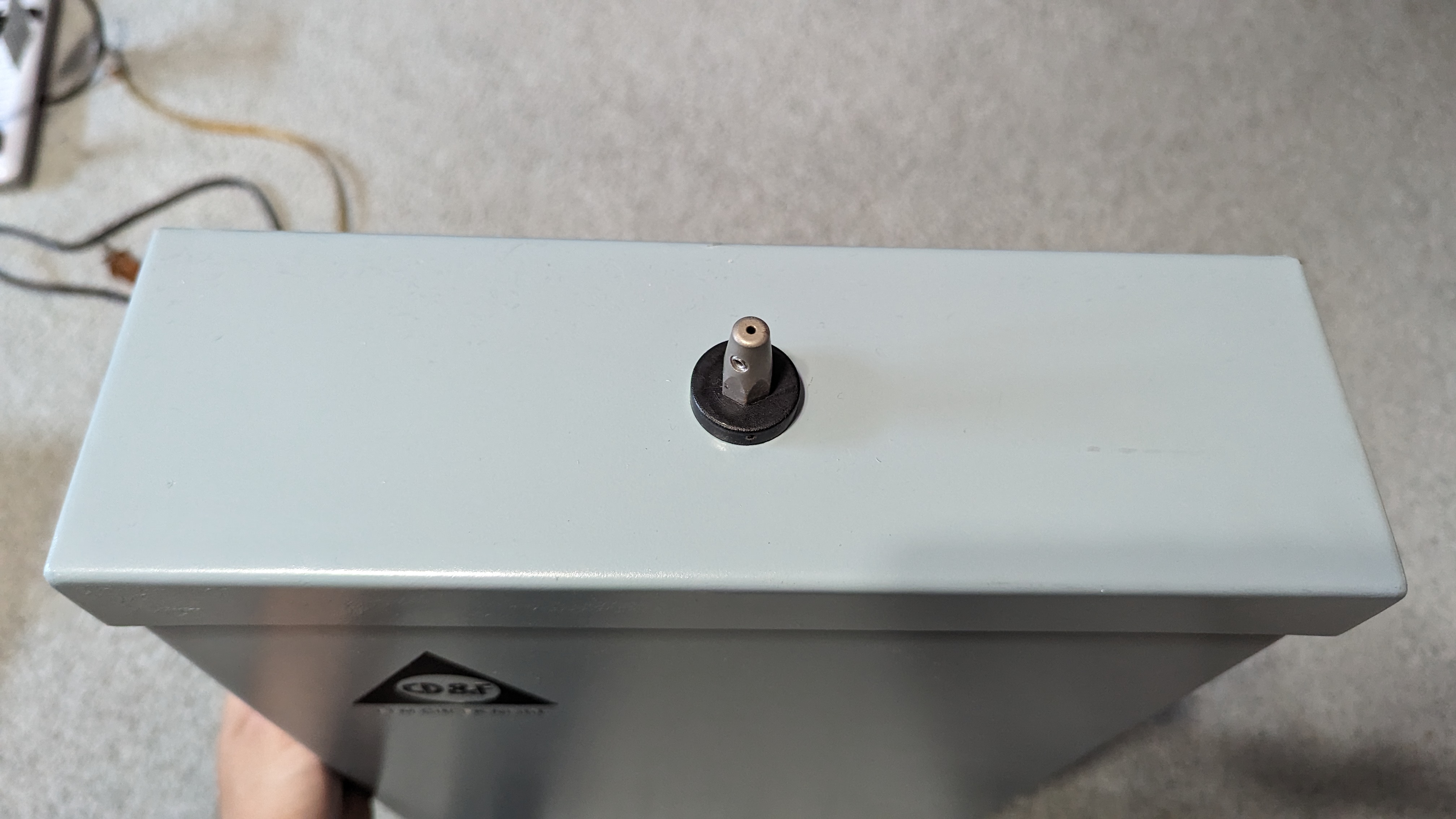
| 18:46, 23 May 2024 | Cdf SC top.jpg (file) |  |
1.46 MB | Top of the SC series CD&F | 1 |
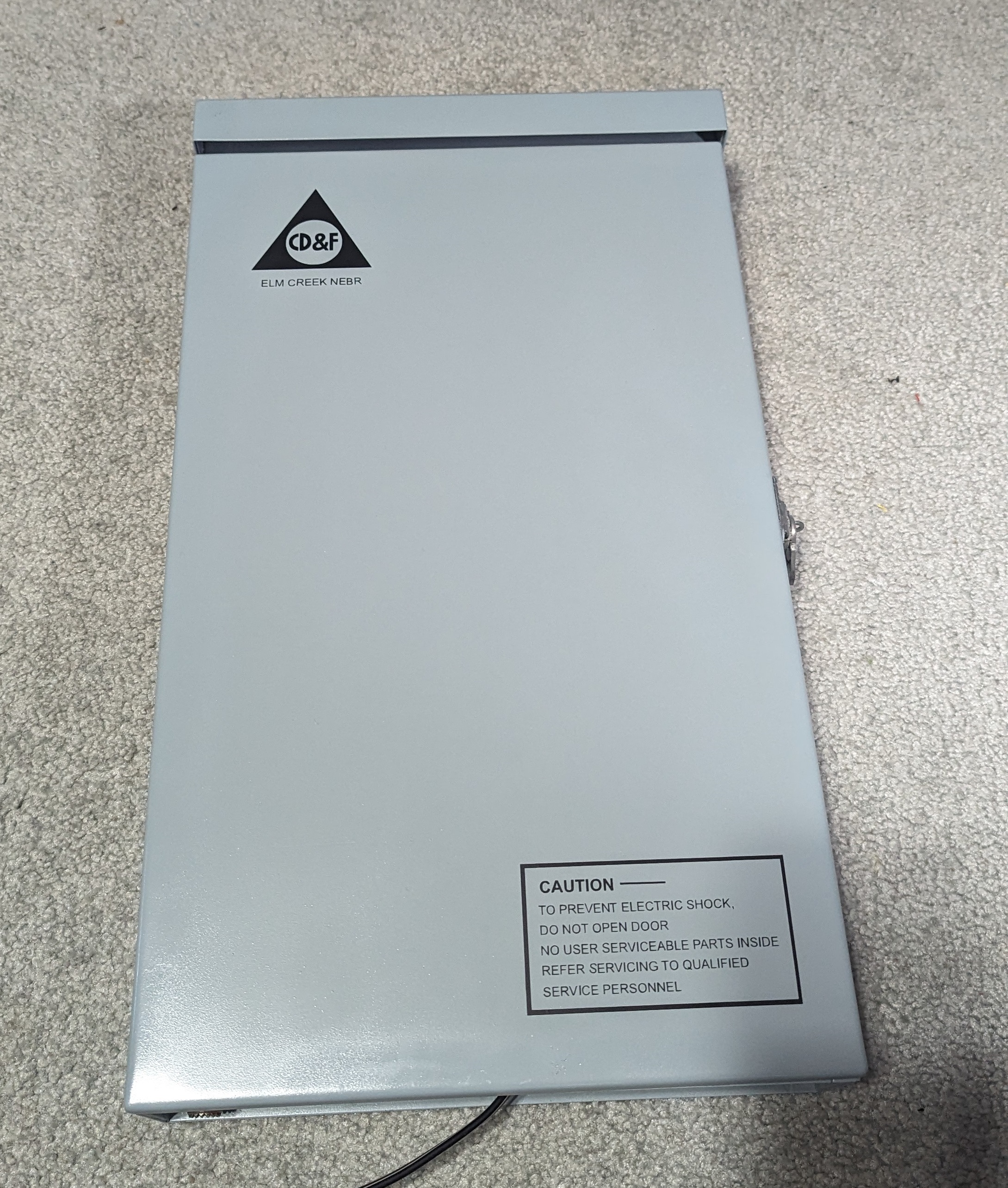
| 18:42, 23 May 2024 | Cdf SC front restored.jpg (file) |  |
1.76 MB | Front of my SC series CD&F after restoration | 1 |
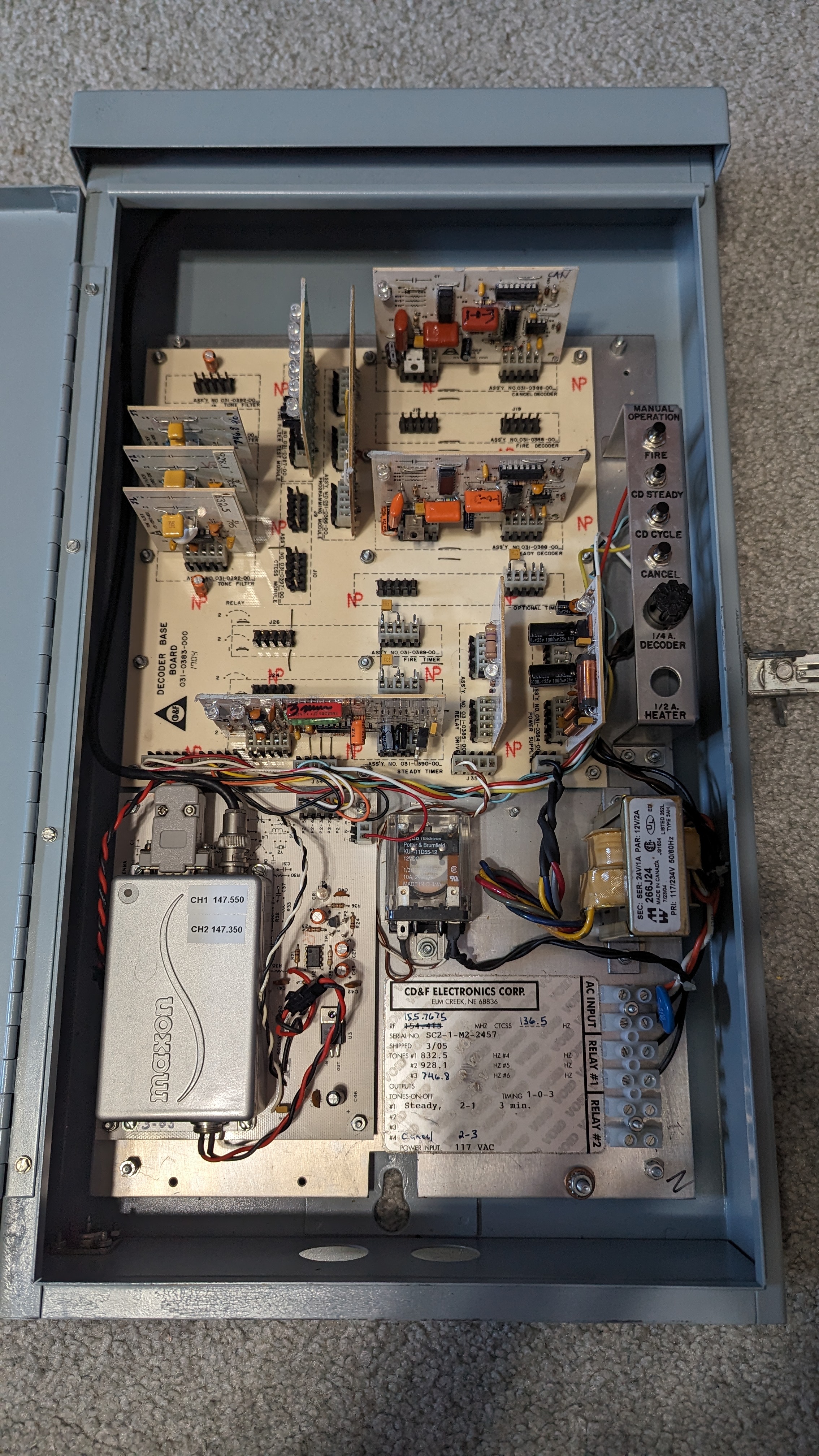
| 18:38, 23 May 2024 | Cdf SC inside.jpg (file) |  |
2.75 MB | Inside of the SC series CD&F after restoration and adding missing control buttons | 1 |
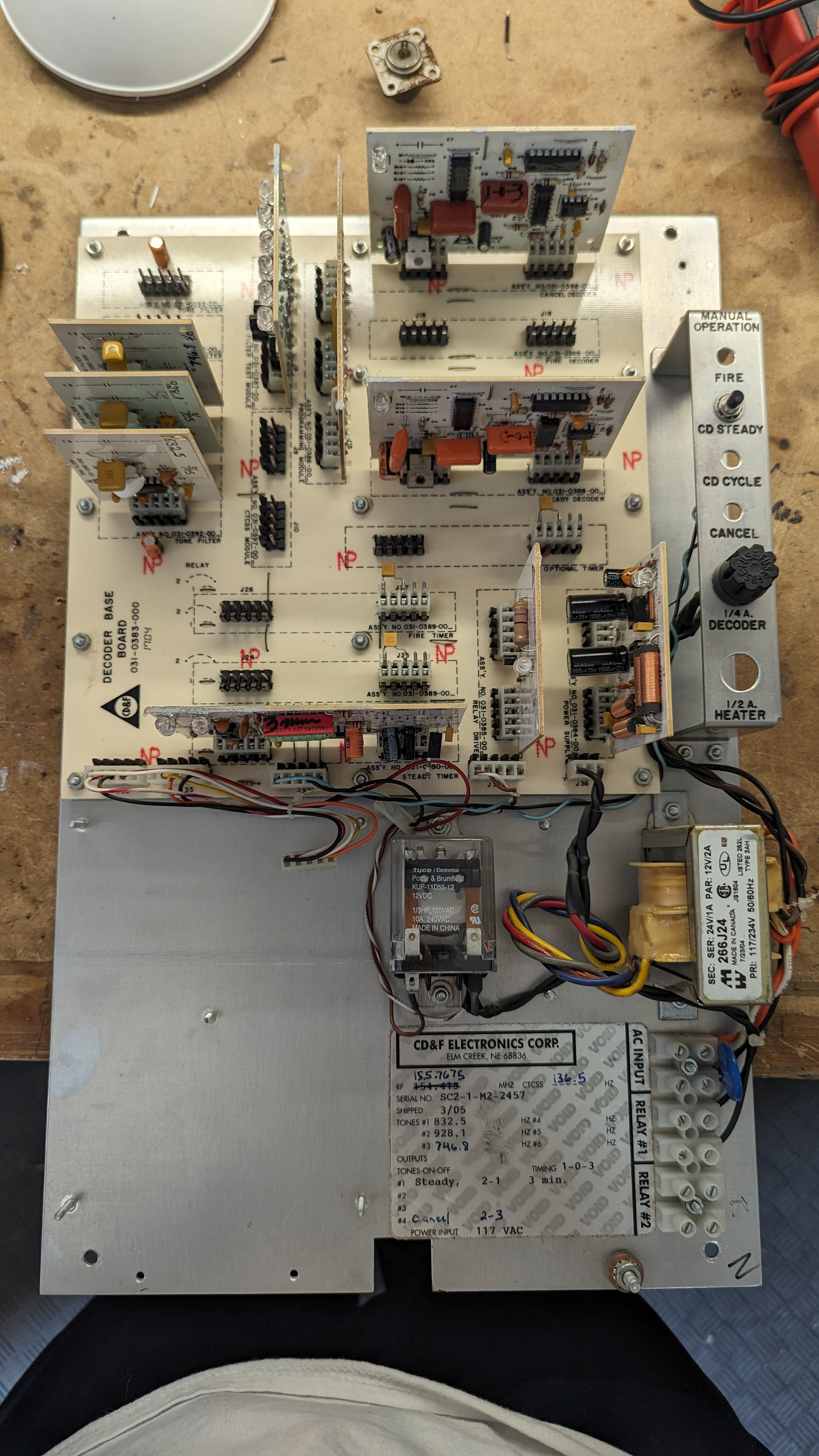
| 02:58, 23 May 2024 | Cdf SC assembly wo radio.jpg (file) |  |
2.13 MB | Sub-assembly of the SC series CD&F without the radio receiver module installed | 1 |
| 02:56, 23 May 2024 | Cdf SC Button conn pinout.png (file) |  |
114 KB | Pinout of the local control header on the SC series CD&F | 1 |
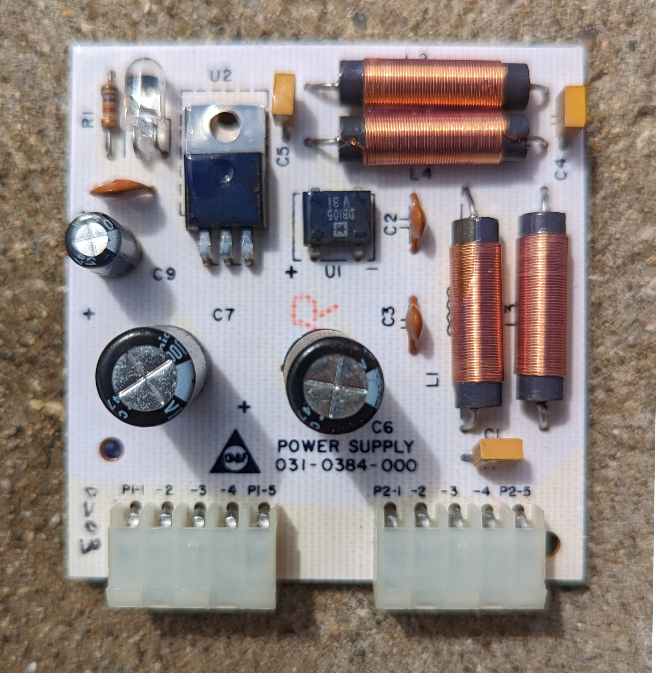
| 02:56, 23 May 2024 | Cdf SC psu module front.jpg (file) |  |
934 KB | Front of the SC series CD&F power supply module | 1 |
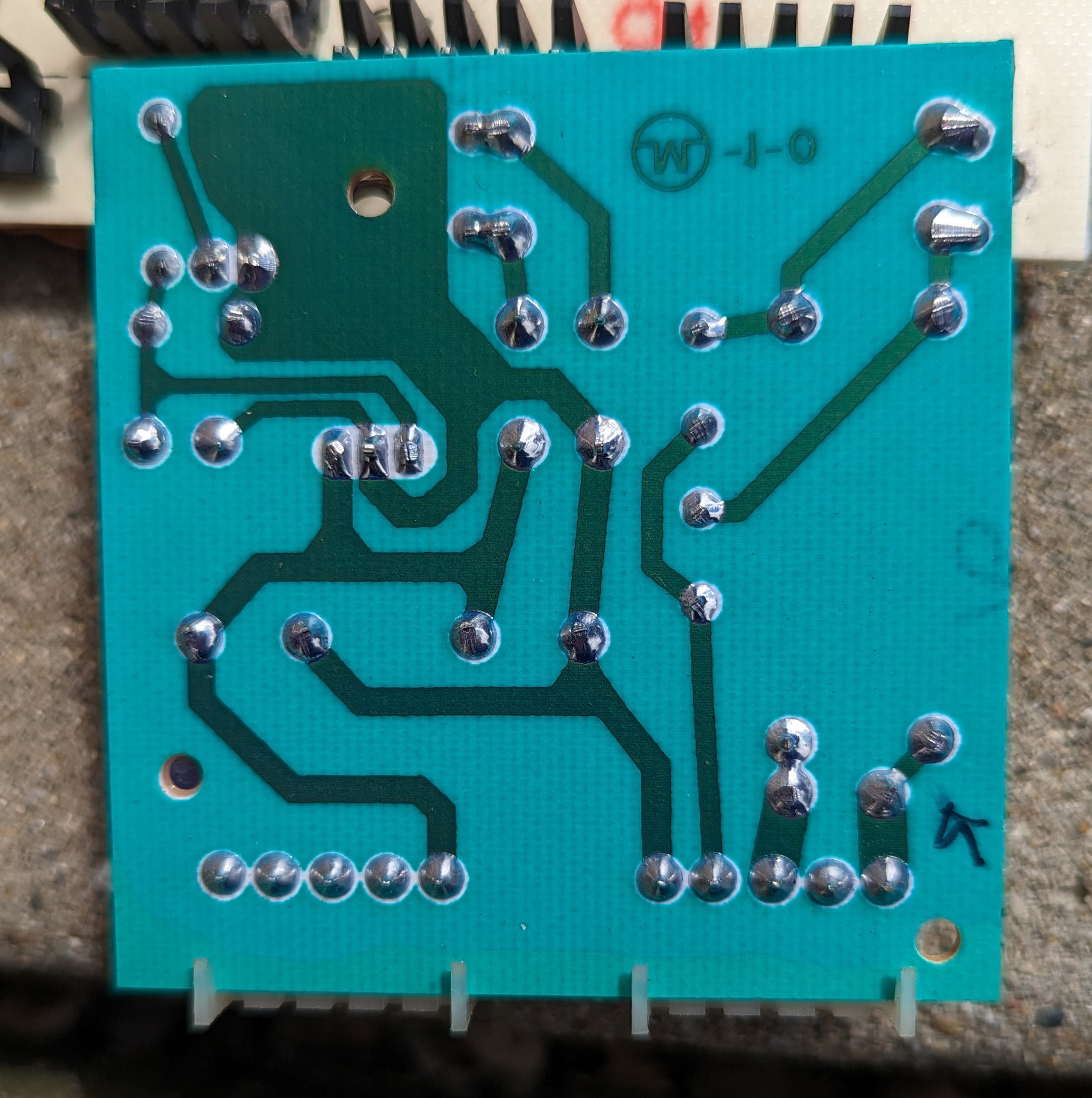
| 02:55, 23 May 2024 | Cdf SC psu back.jpg (file) |  |
843 KB | Rear of the SC series CD&F power supply module | 1 |
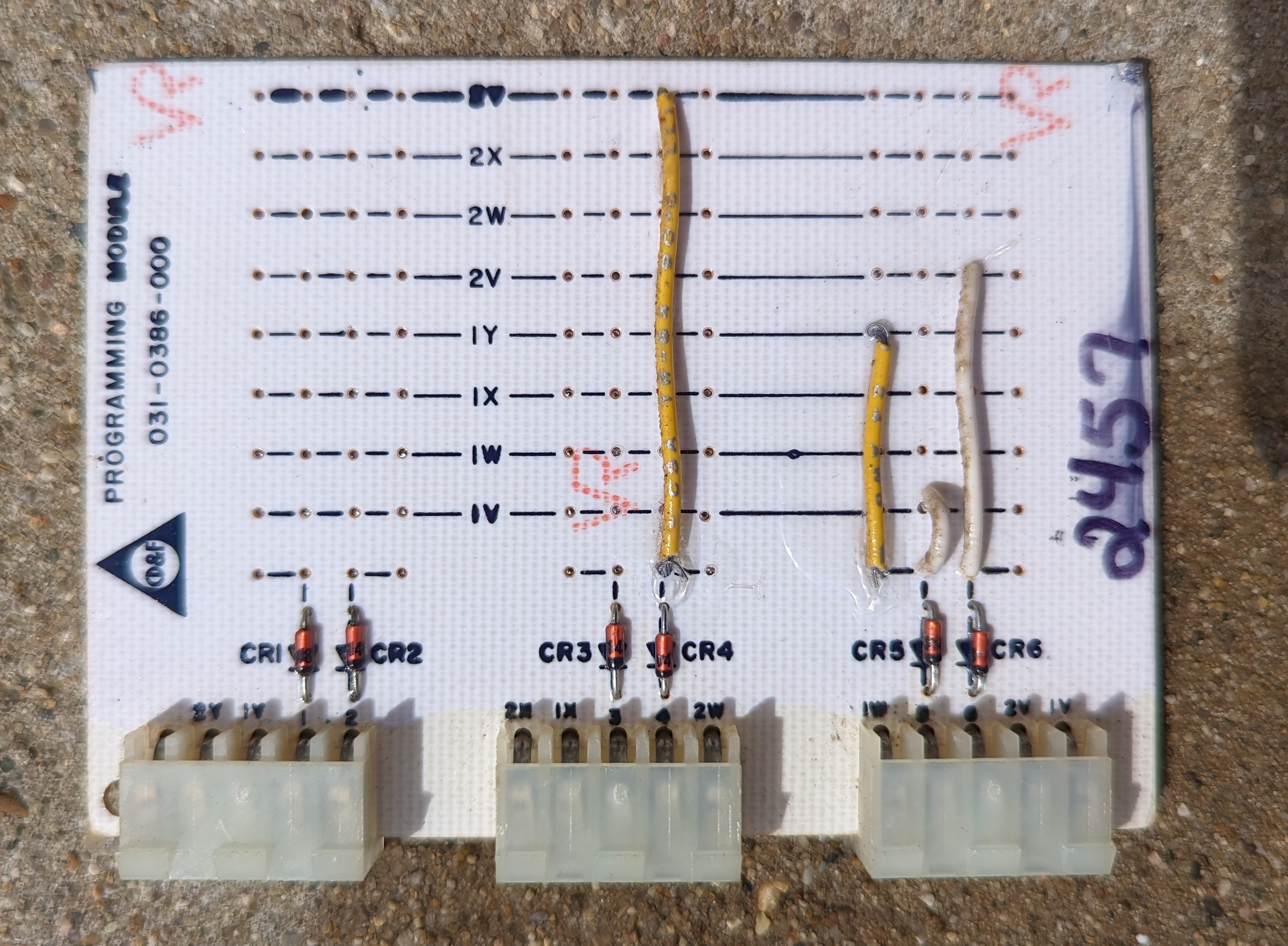
| 02:54, 23 May 2024 | Cdf SC prog module front.jpg (file) |  |
1.15 MB | Front of the SC series CD&F programming module | 1 |
| 02:54, 23 May 2024 | Cdf SC prog module back.jpg (file) |  |
1.32 MB | Rear of the SC series CD&F programming module | 1 |
| 02:53, 23 May 2024 | Cdf SC front case.jpg (file) |  |
1.09 MB | Front case of my SC series unit before restoration. The logo was penciled in by me for measurement and recreation | 1 |
| 02:53, 23 May 2024 | Cdf SC decodertester rear.jpg (file) |  |
1.61 MB | Rear of the decoder tester board from the SC series CD&F | 1 |
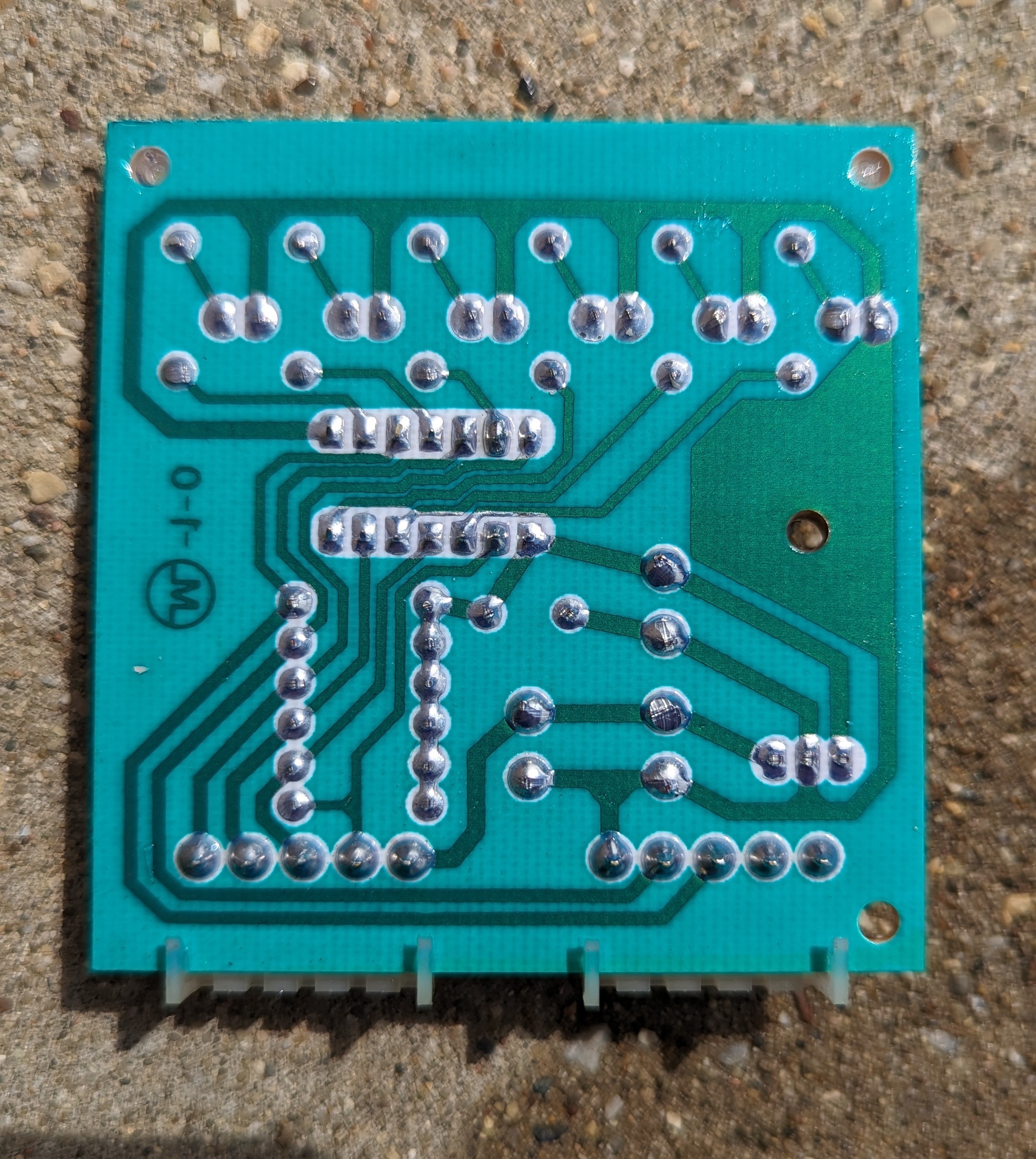
| 02:52, 23 May 2024 | Cdf SC decodertester front.jpg (file) |  |
1.63 MB | Front of the decoder tester board from the SC series CD&F | 1 |
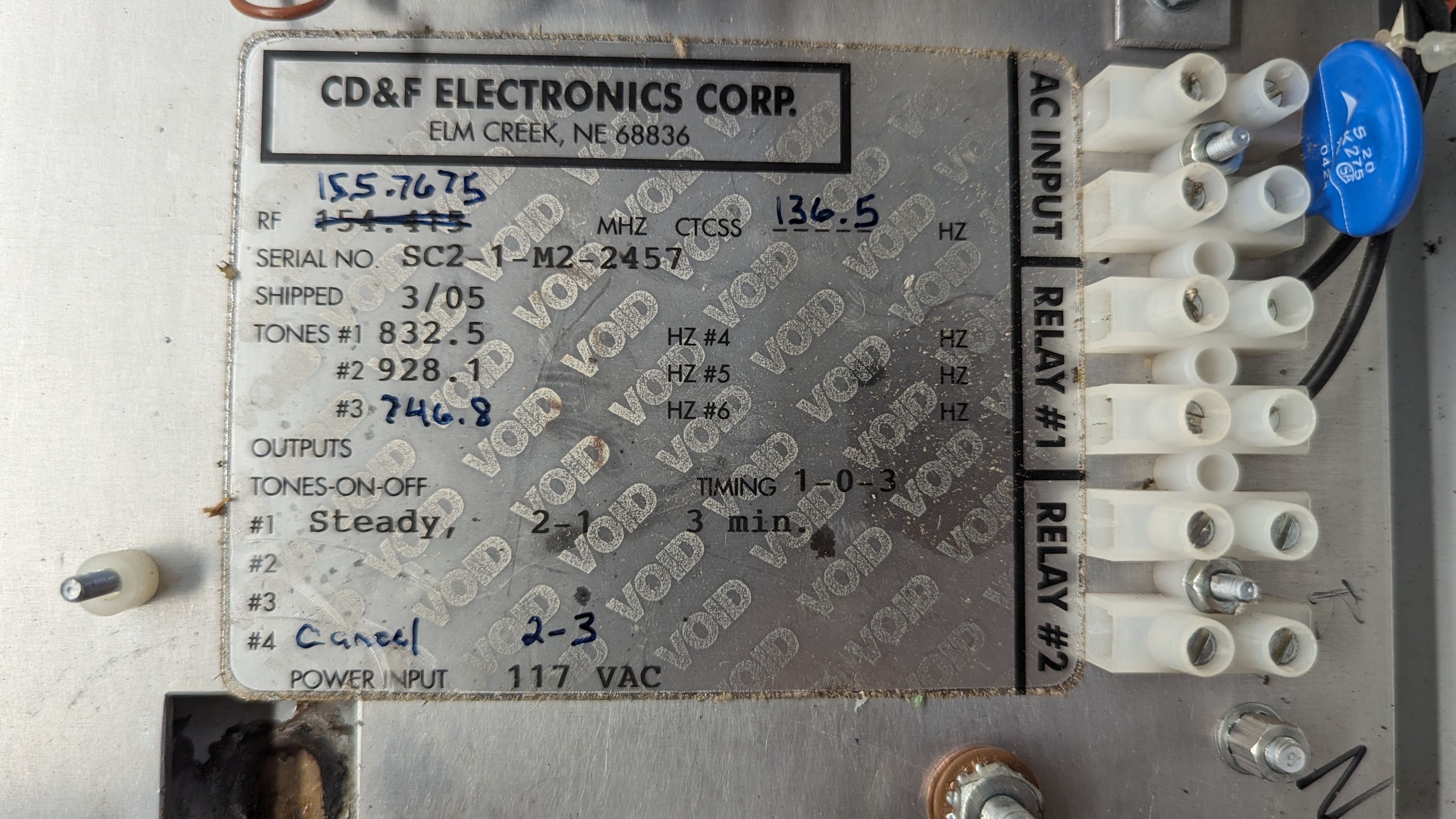
| 02:39, 23 May 2024 | Cdf SC nameplate.jpg (file) |  |
1.27 MB | Nameplate of the larger SC series CD&F controller | 1 |
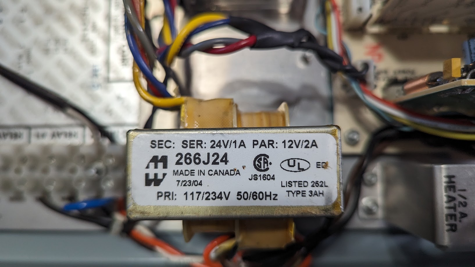
| 23:34, 21 May 2024 | Cdf SC transformer details.jpg (file) | 212 KB | CD&F SC series transformer detailed close-up | 1 | |
| 23:33, 21 May 2024 | Toroid1.gif (file) |  |
3 KB | Hammond 266J24 transformer pinout from https://www.hammfg.com/electronics/transformers/power/266 | 1 |
| 02:44, 15 May 2024 | Maxon sd 161.jpg (file) |  |
204 KB | Maxon SD-161 data radio installed in a CD&F siren controller | 1 |
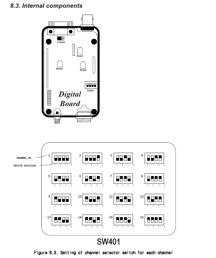
| 23:50, 14 May 2024 | Maxon DIP switch config.png (file) |  |
42 KB | Channel selection diagram for maxon data radios | 1 |
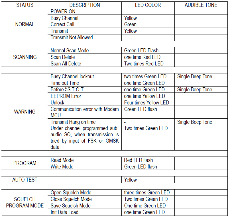
| 23:43, 14 May 2024 | Maxon radio status chart.png (file) |  |
60 KB | Status chart from Maxon radio service manual | 1 |
| 23:29, 14 May 2024 | Acc2016 schematic.png (file) |  |
54 KB | Schematic for the model ACC-2016 programming cable for Maxon data radios | 1 |
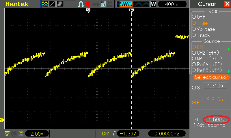
| 06:43, 26 April 2024 | Cdf timer rc scope2.png (file) |  |
17 KB | Scope view of the RC oscillator on the CD&F Timer | 1 |
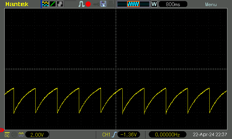
| 06:42, 26 April 2024 | Cdf timer RC scope.png (file) |  |
26 KB | Scope view of the RC oscillator on the CD&F Timer | 1 |
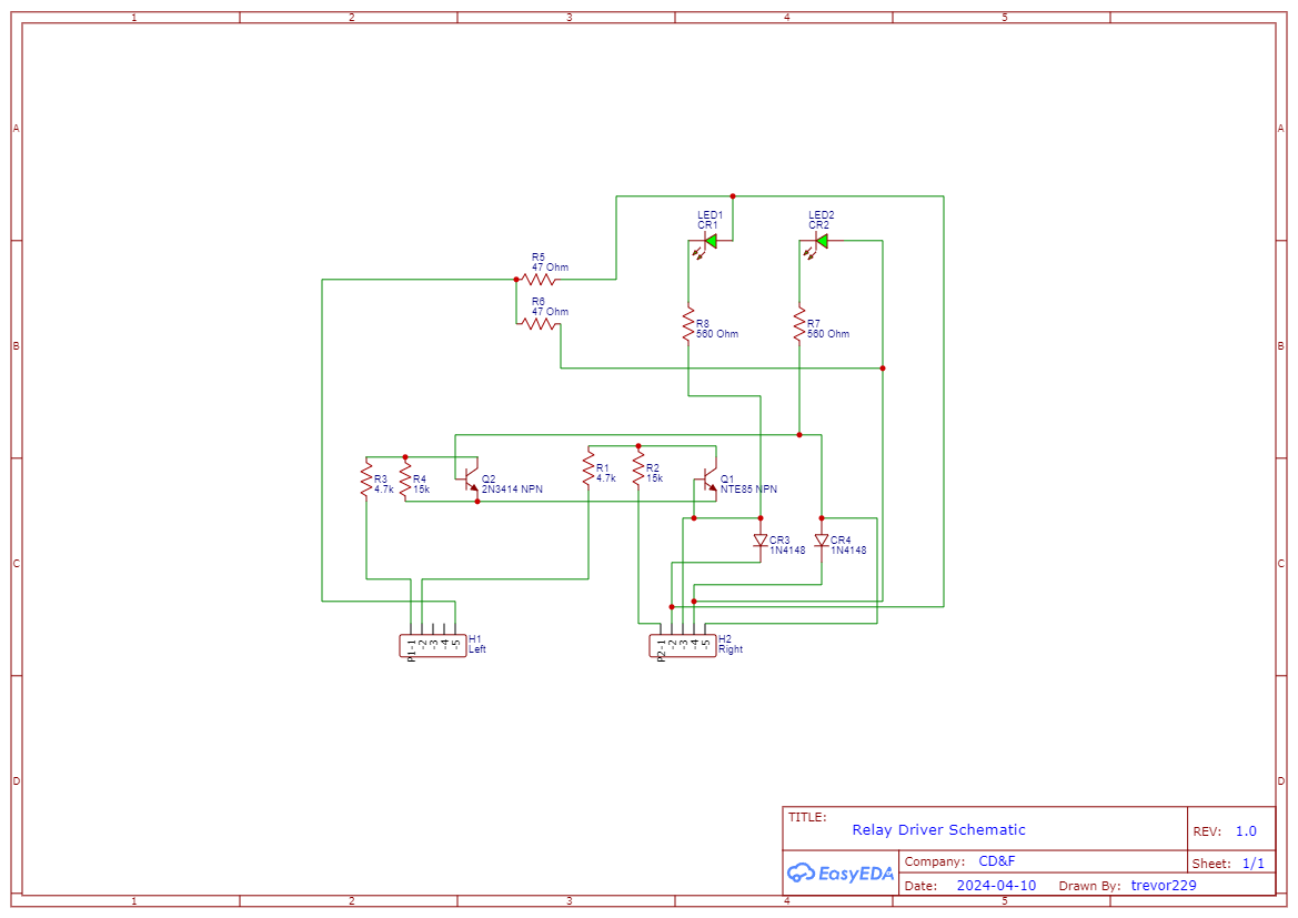
| 00:15, 17 April 2024 | Cdf relay driver schematic.png (file) |  |
53 KB | (Hopefully correct) schematic of the CD&F relay driver board | 1 |
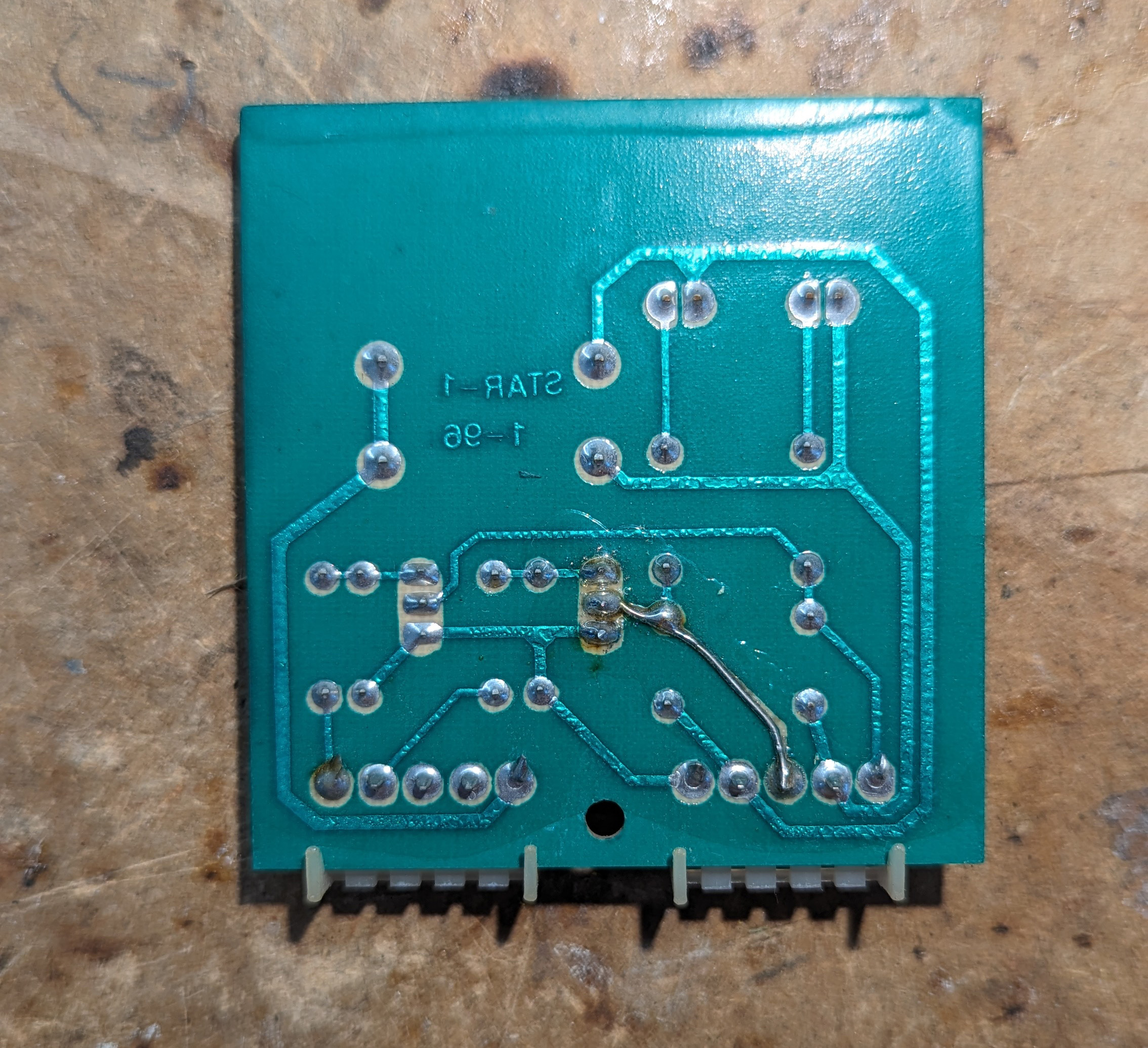
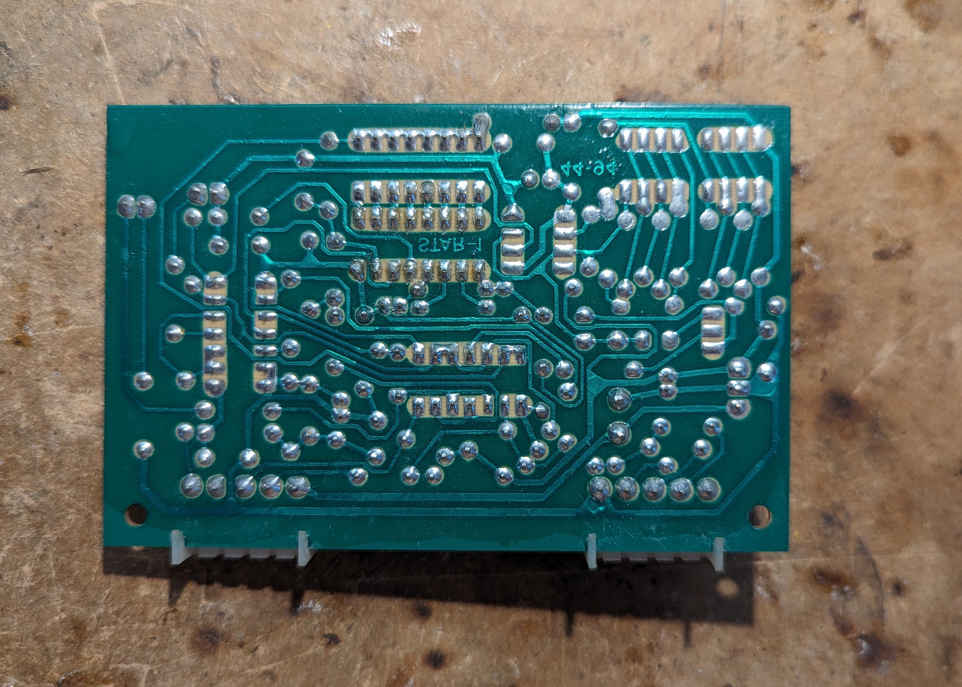
| 00:14, 17 April 2024 | Cdf relay driver back.jpg (file) |  |
1.17 MB | Backside of the relay driver board for the CD&F | 1 |
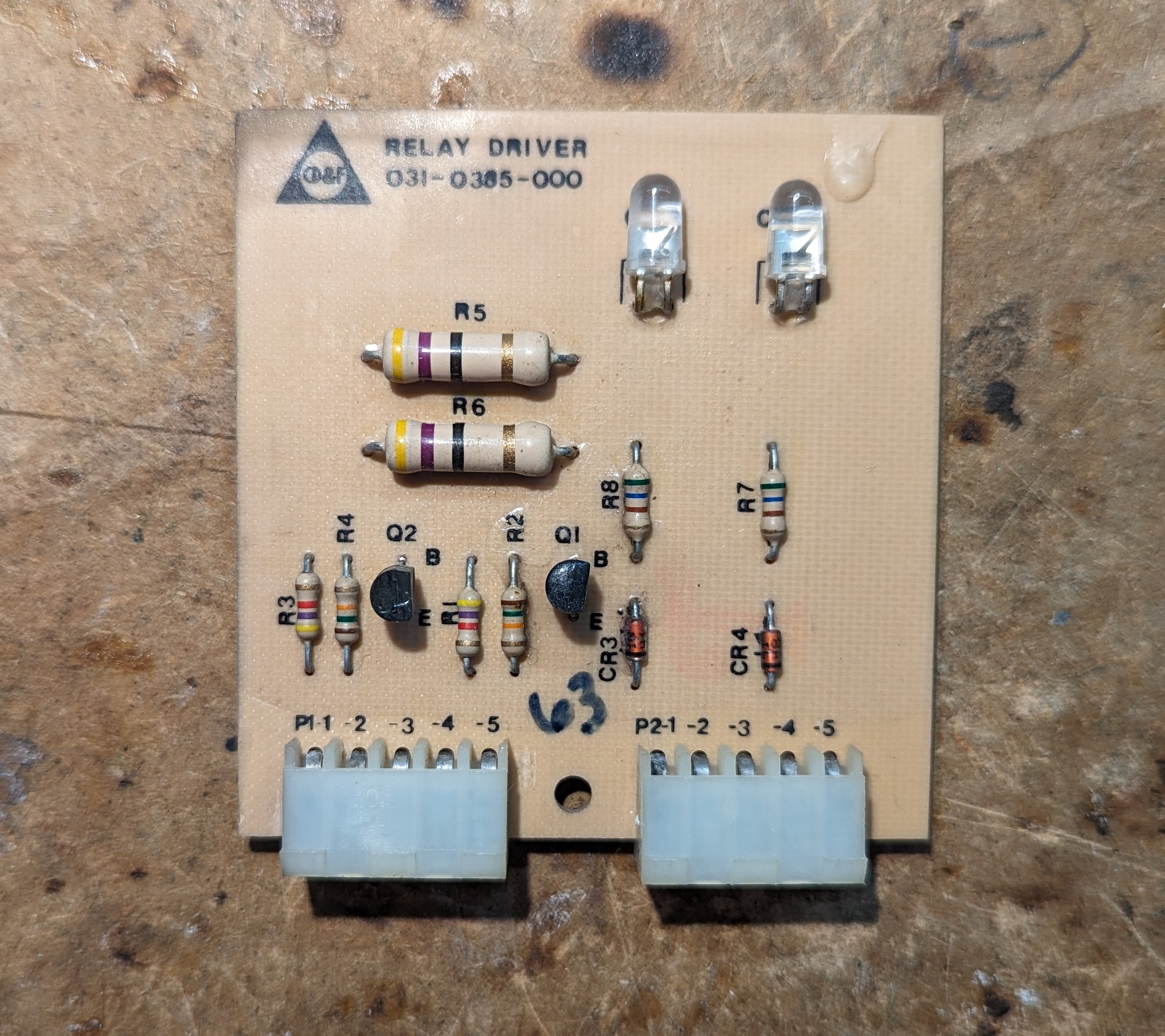
| 00:13, 17 April 2024 | Cdf relay driver top.jpg (file) |  |
1.32 MB | Relay driver board from the CD&F | 1 |
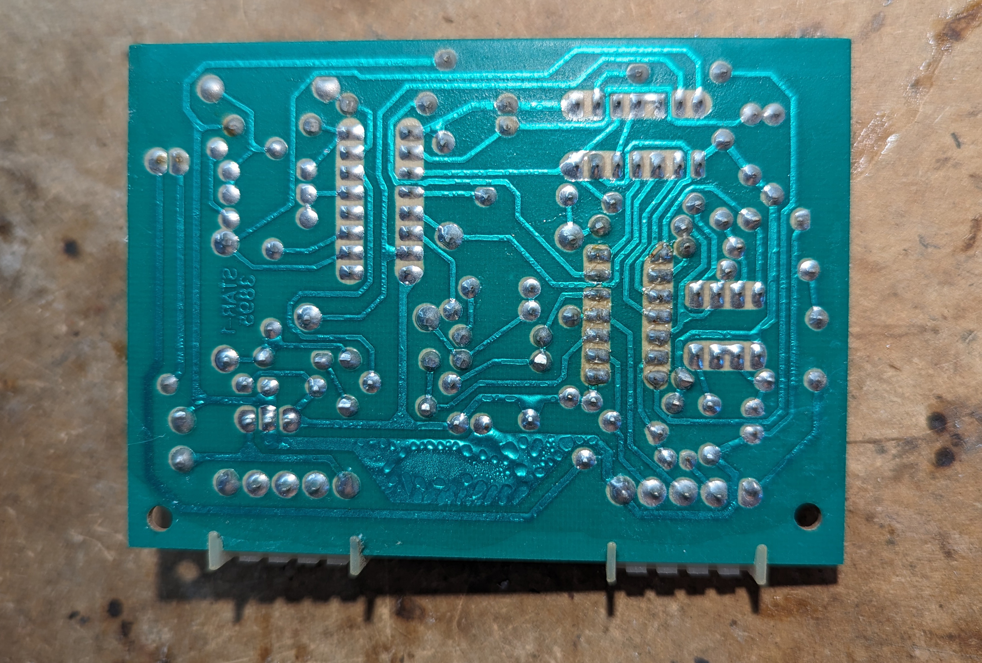
| 00:10, 17 April 2024 | Cdf cycle timer back.jpg (file) |  |
1.91 MB | Cycle timer (Steady) backside (Mirrored to match Cdf_cycle_timer_front.jpg) | 1 |
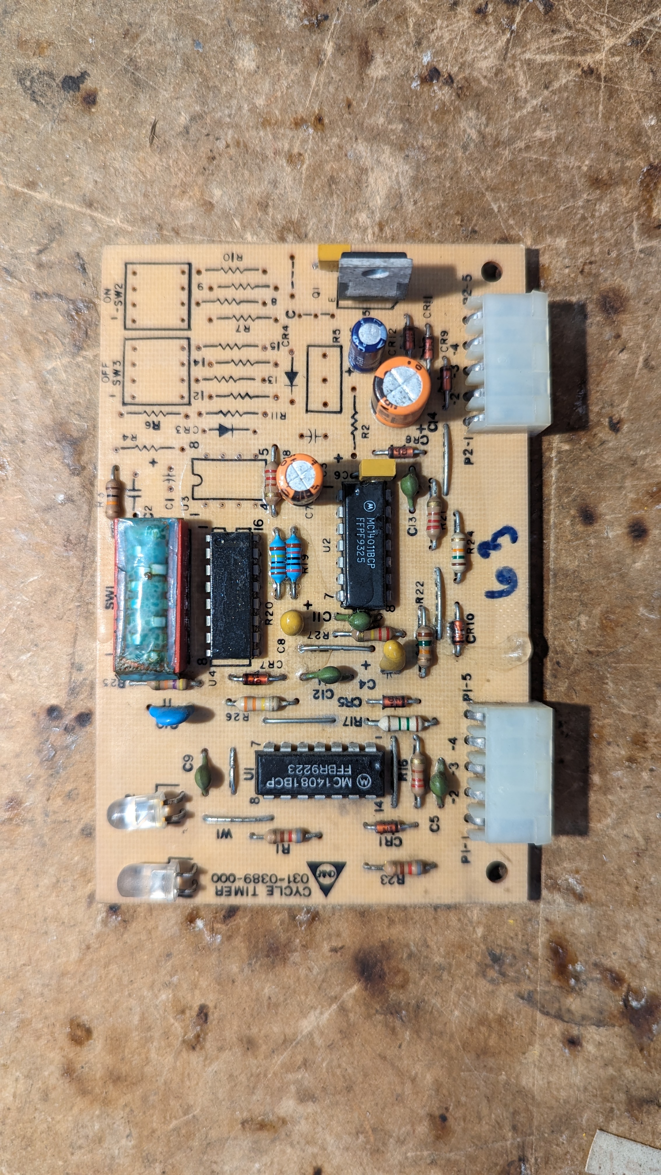
| 00:09, 17 April 2024 | Cdf cycle timer front.jpg (file) |  |
2.58 MB | Cycle timer (Steady) front from the CD&F | 1 |
| 00:09, 17 April 2024 | Cdf decoder module a back.jpg (file) |  |
1.67 MB | Backside of the tone decoder module from the CD&F (Mirrored to match Cdf_decoder_module_a_front.jpg | 1 |
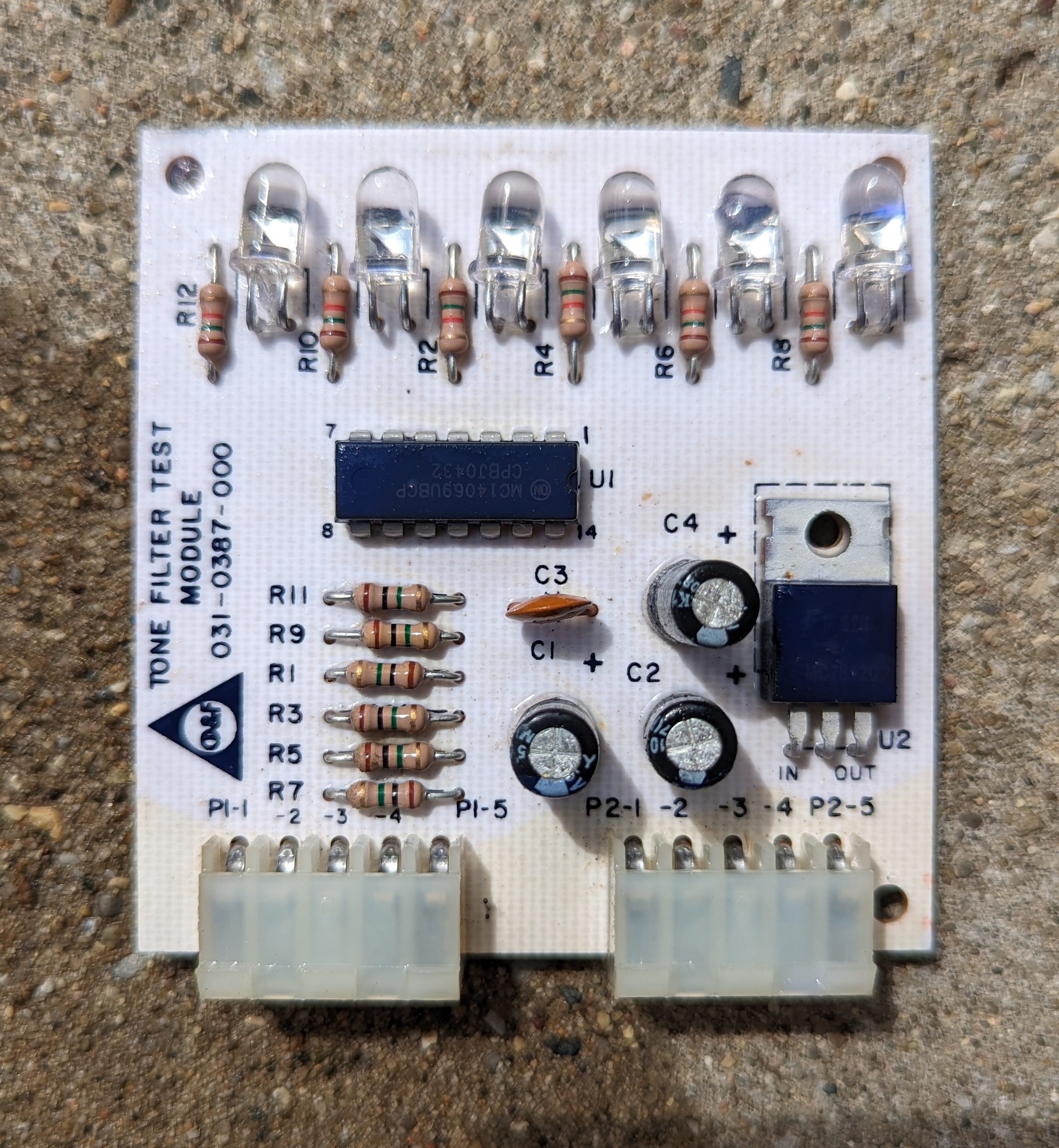
| 00:07, 17 April 2024 | Cdf decoder module a front.jpg (file) |  |
1.94 MB | Front of the tone decoder module from the CD&F | 1 |
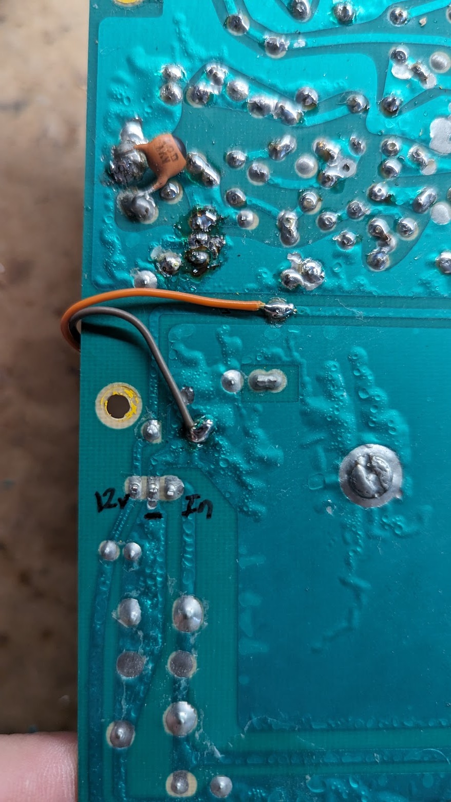
| 03:25, 16 April 2024 | Cdf mod power connections.jpg (file) |  |
364 KB | Connections for Vin and GND to power the arduino and Si5351 board on the CD&F. Pulling power from the main 12v regulator | 1 |
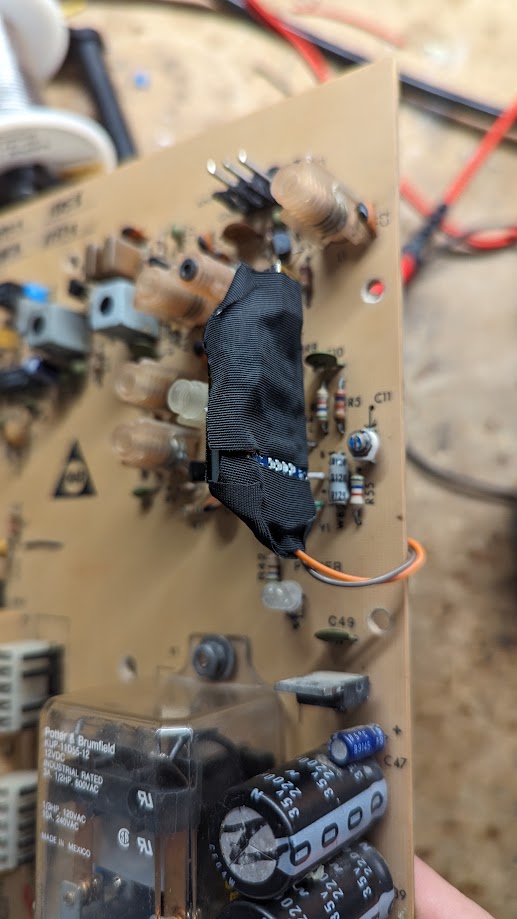
| 03:24, 16 April 2024 | Cdf modded LO.jpg (file) |  |
98 KB | Final mod showing the insulated arduino and Si5351 board attached to the CD&F main board | 1 |
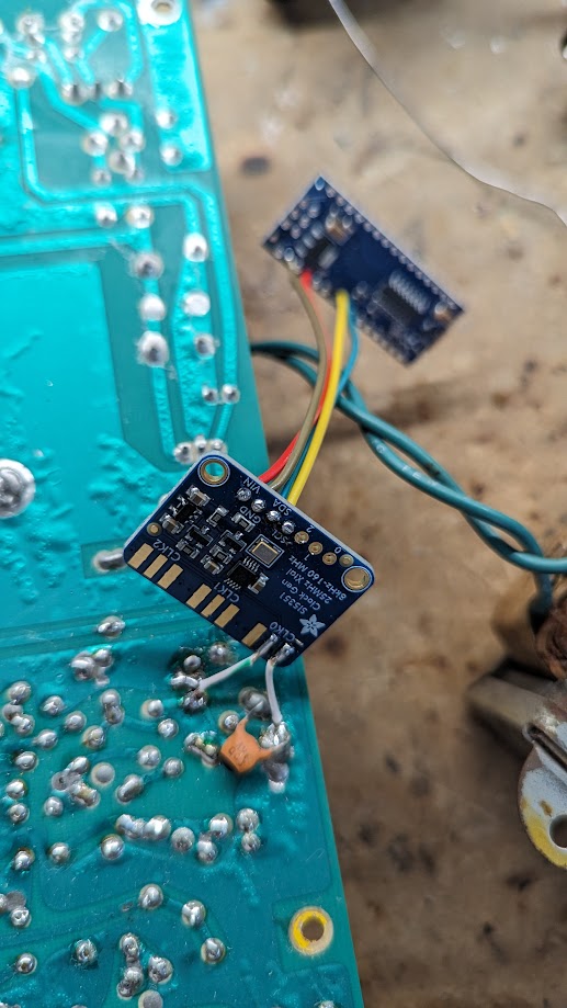
| 03:21, 16 April 2024 | Cdf si5351 test.jpg (file) |  |
123 KB | Test setup of the Si5351 breakout board to replace the LO crystal on the CD&F | 1 |
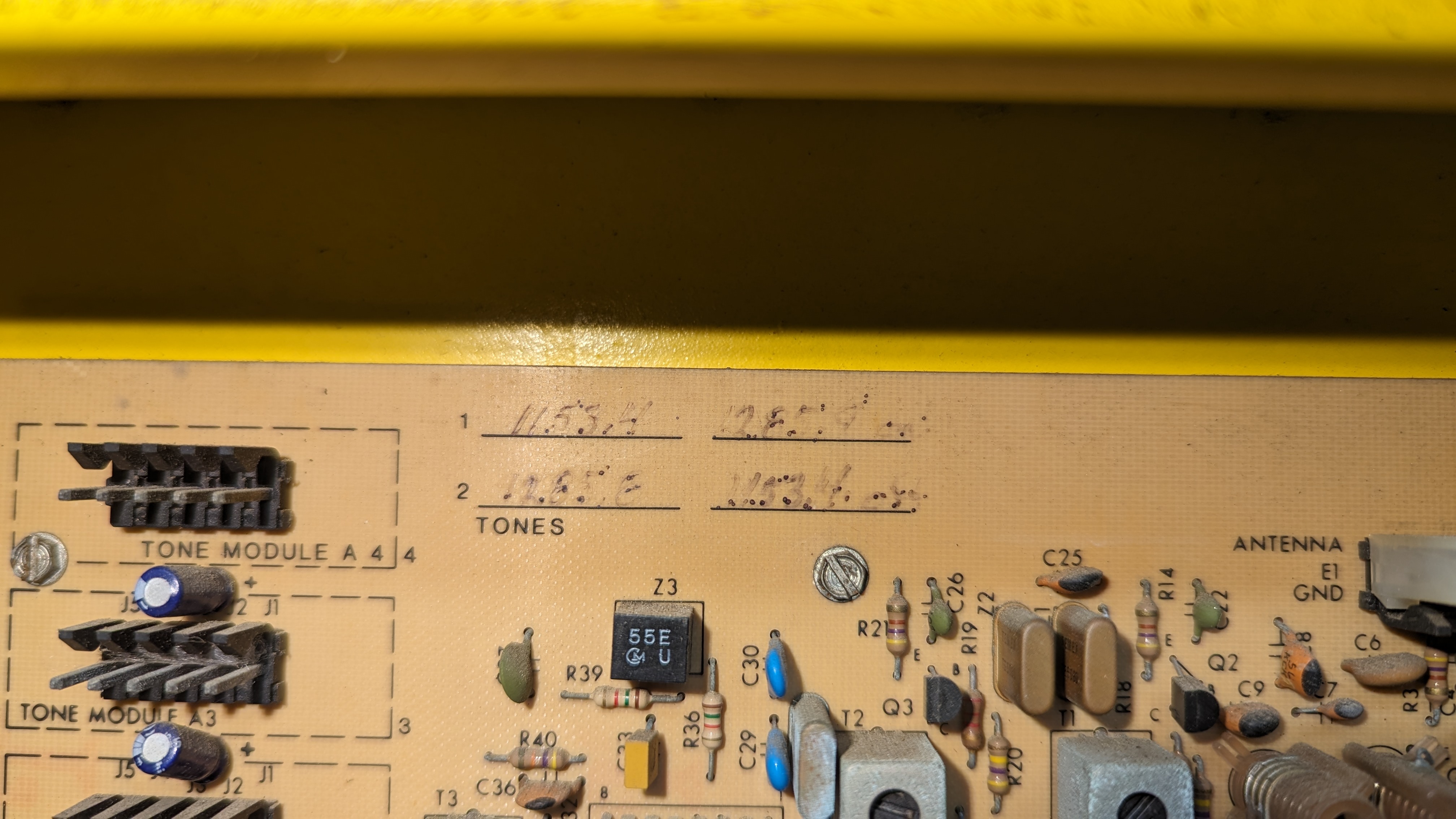
| 23:26, 15 April 2024 | Cdf tone info.jpg (file) |  |
1.46 MB | Configured tone information handwritten on the CD&F main board near the top center. Sequence 1 is to activate, sequence 2 is to deactivate. | 1 |
| 23:23, 15 April 2024 | Cdf rx closeup back.jpg (file) |  |
2.15 MB | Closeup of the rear of the double conversion super heterodyne radio receiver circuitry in the CD&F. Mirrored to match Cdf_rx_closeup.jpg | 1 |
| 23:22, 15 April 2024 | Cdf rx closeup.jpg (file) |  |
1.94 MB | Closeup of the double conversion super heterodyne radio receiver circuitry in the CD&F | 1 |
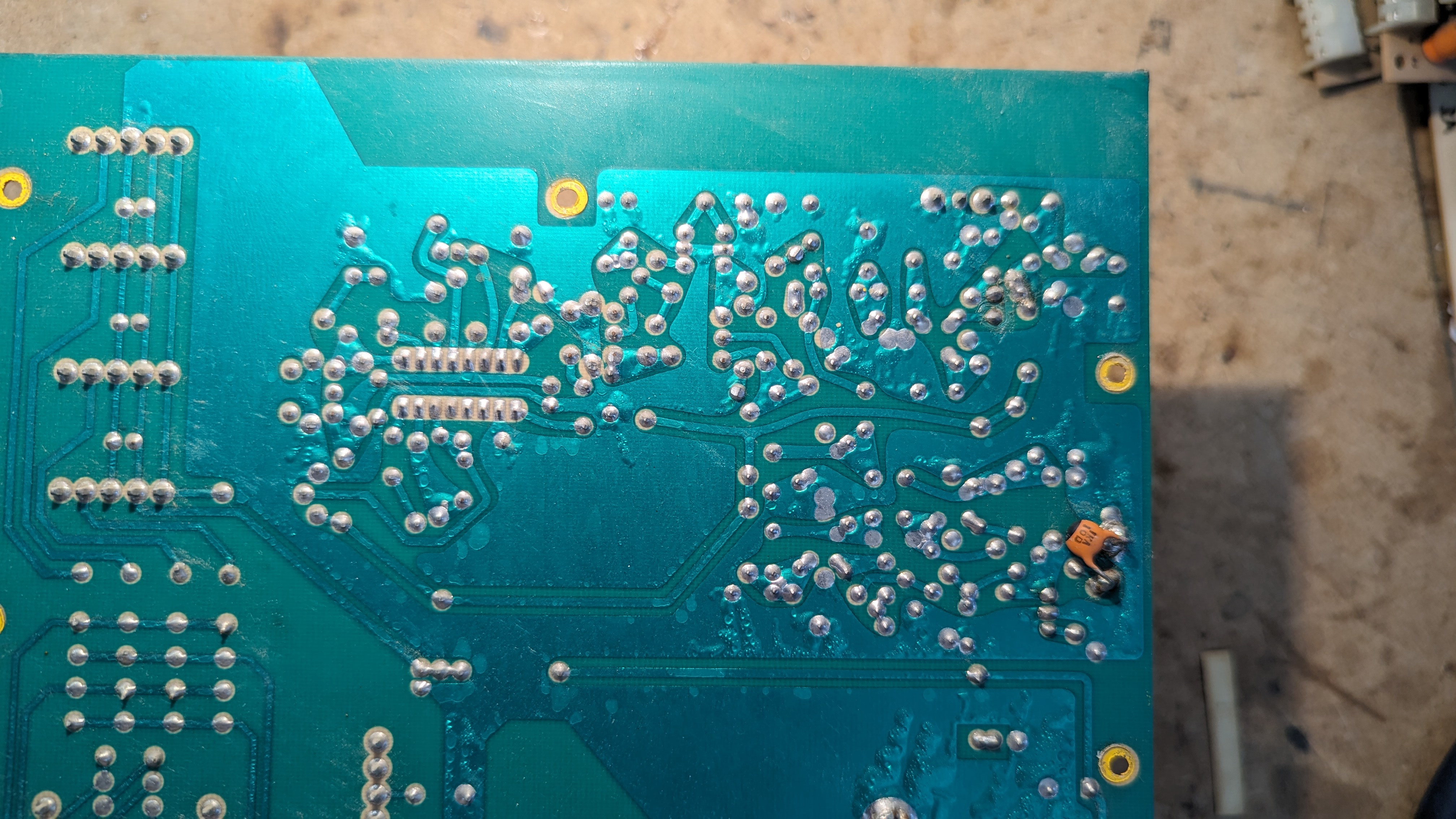
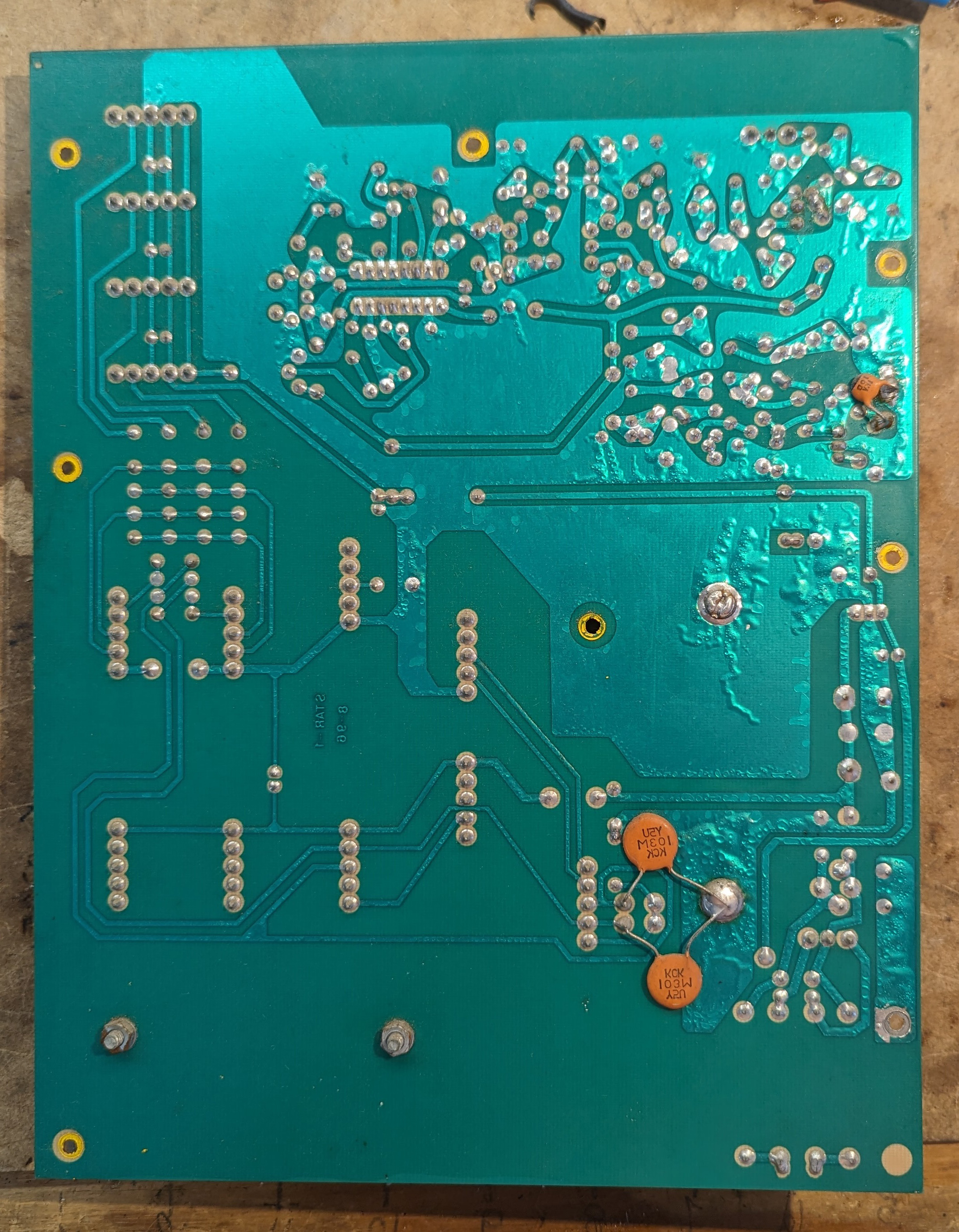
| 23:21, 15 April 2024 | Cdf bare mainboard back.jpg (file) |  |
1.48 MB | Flipped horizontally to match Cdf_bare_mainboard.jpg | 2 |
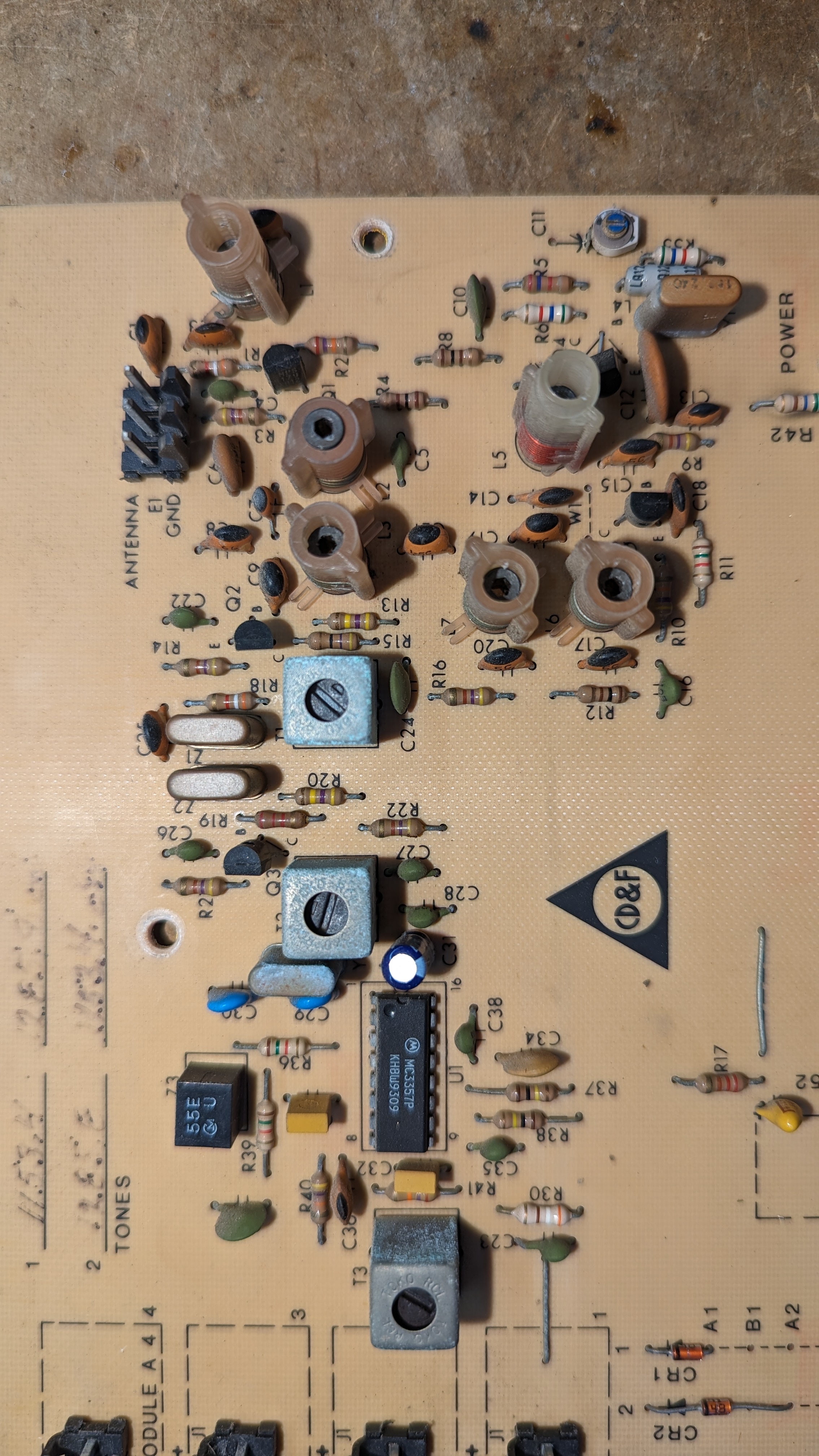
| 23:16, 15 April 2024 | Cdf bare mainboard.jpg (file) |  |
1.96 MB | Bare mainboard of the CD&F. All cards removed for visibility. | 1 |
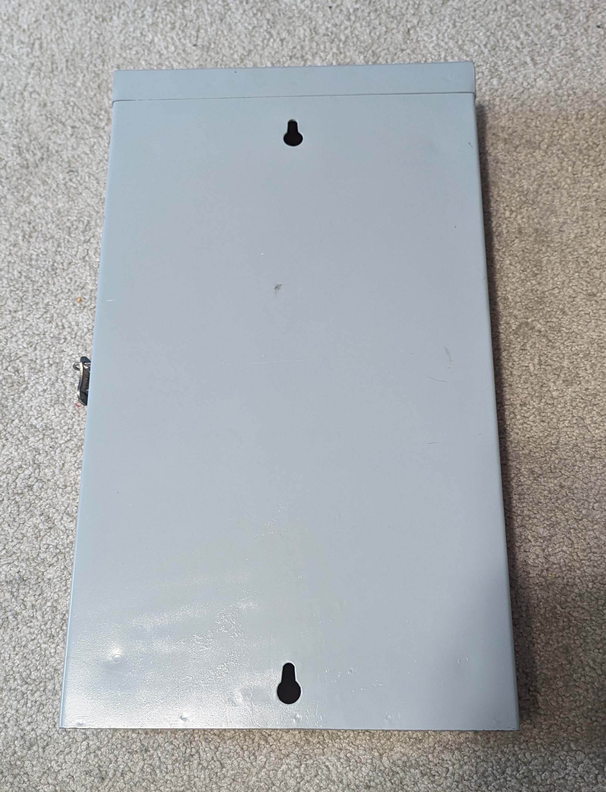
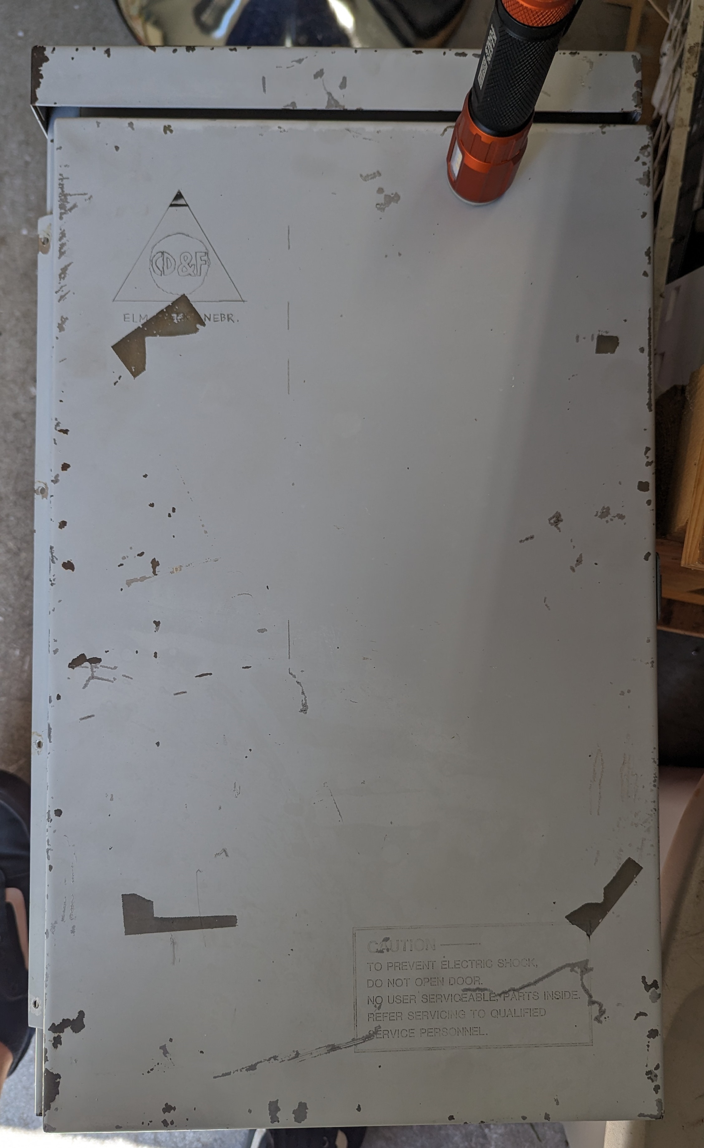
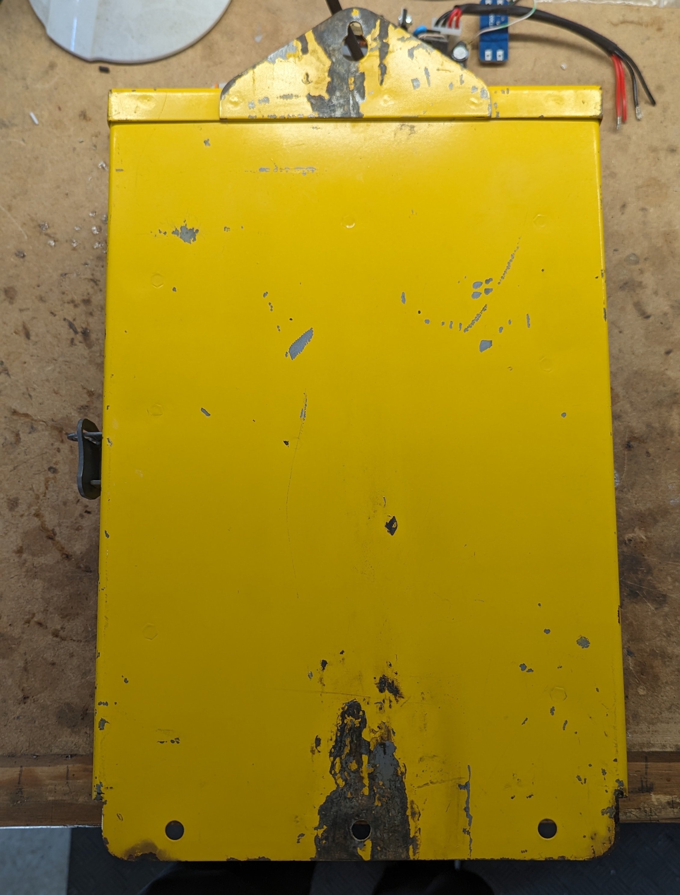
| 23:14, 15 April 2024 | Cdf back.jpg (file) |  |
1,002 KB | Back of the enclosure, showing the integrated mounting holes. | 1 |
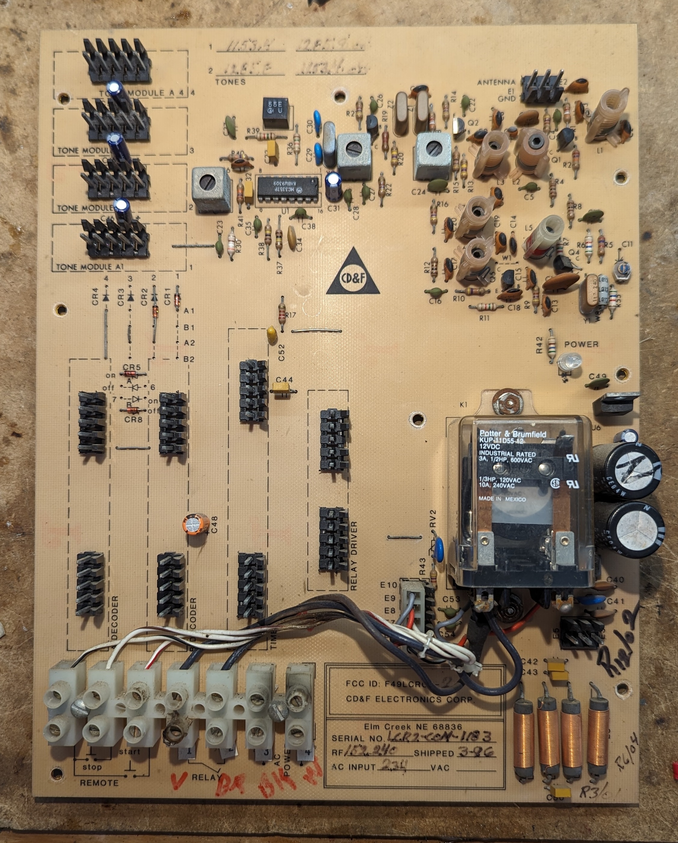
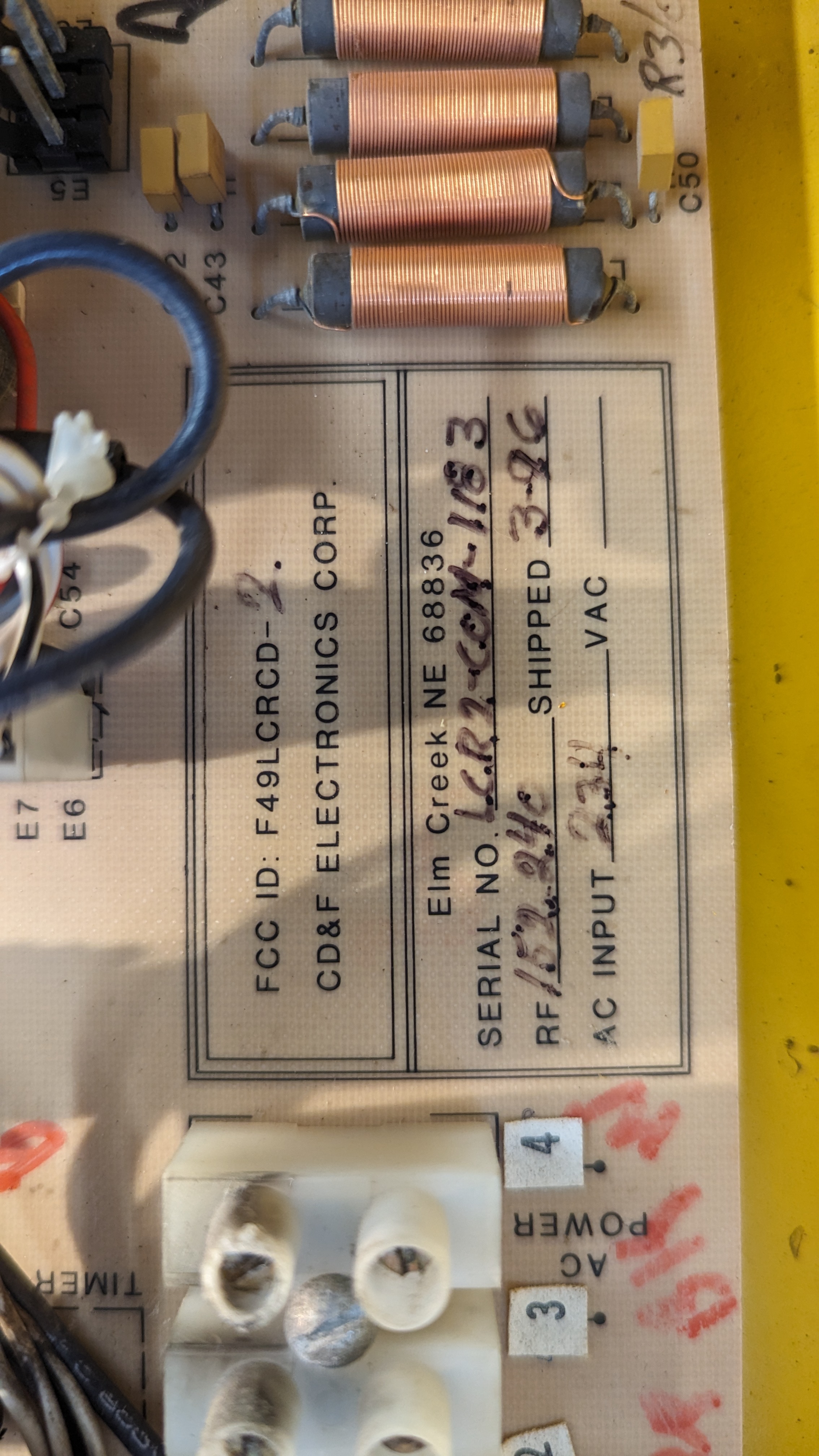
| 23:13, 15 April 2024 | Cdf info onboard.jpg (file) |  |
1.79 MB | Info written near the bottom center of the mainboard. Shows FCC-ID, serial, receive frequency, input voltage, and ship date. | 1 |
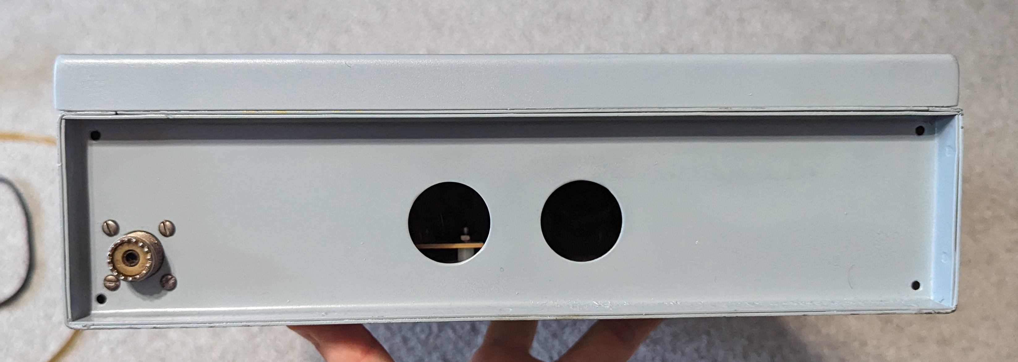
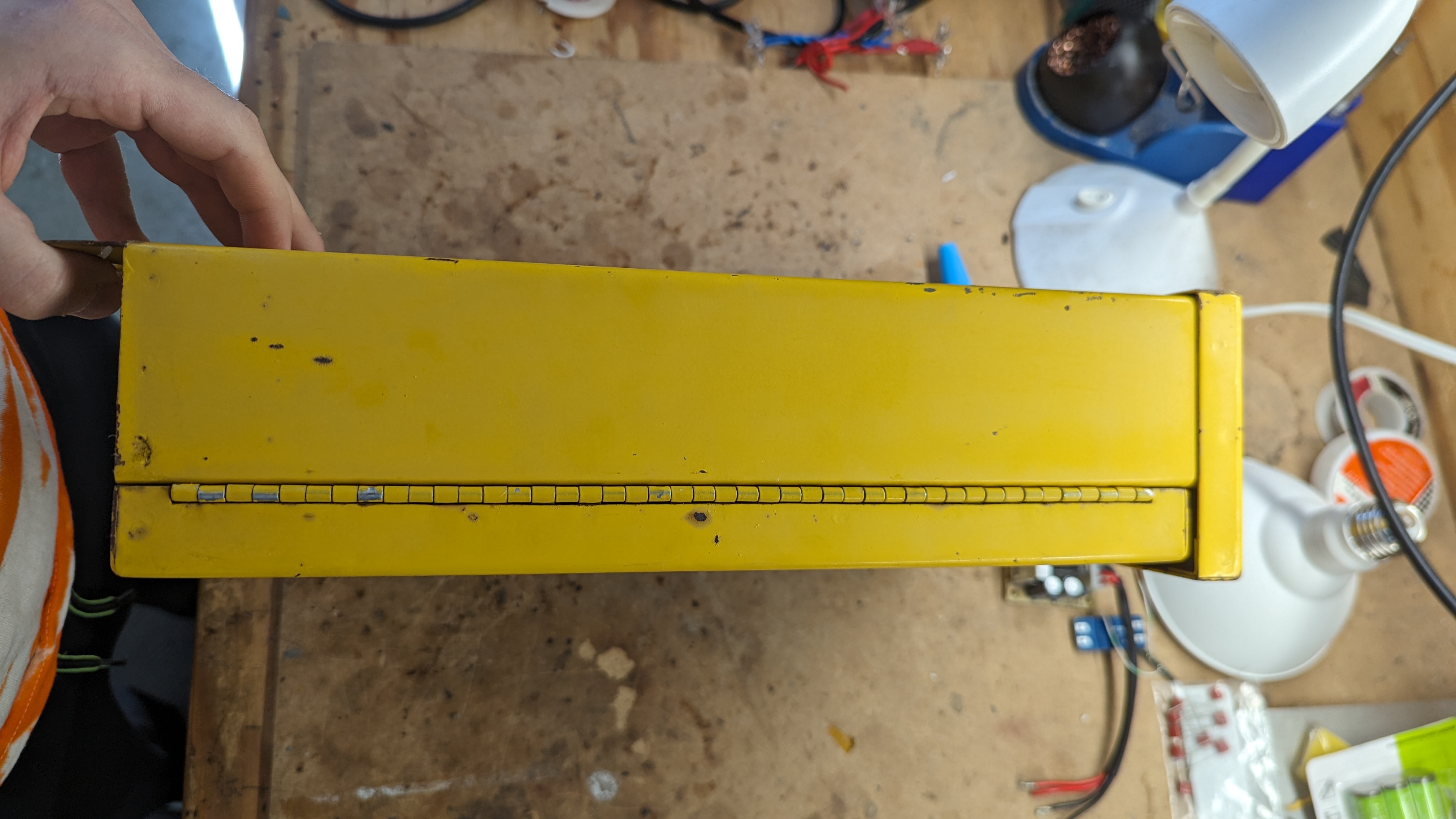
| 23:11, 15 April 2024 | Cdf hinge side.jpg (file) |  |
1.24 MB | Side of the enclosure with the hinge. The hinge cannot be removed from the door, but the door and hinge can be removed from the enclosure with three screws and nuts. | 1 |
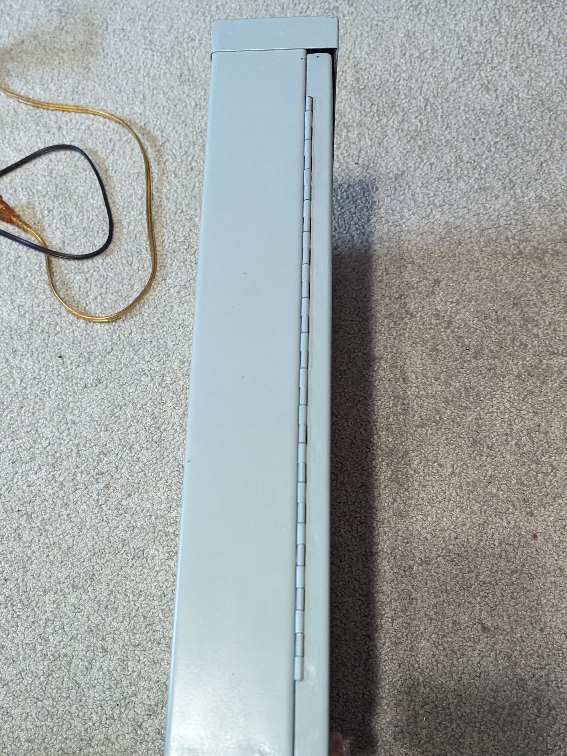
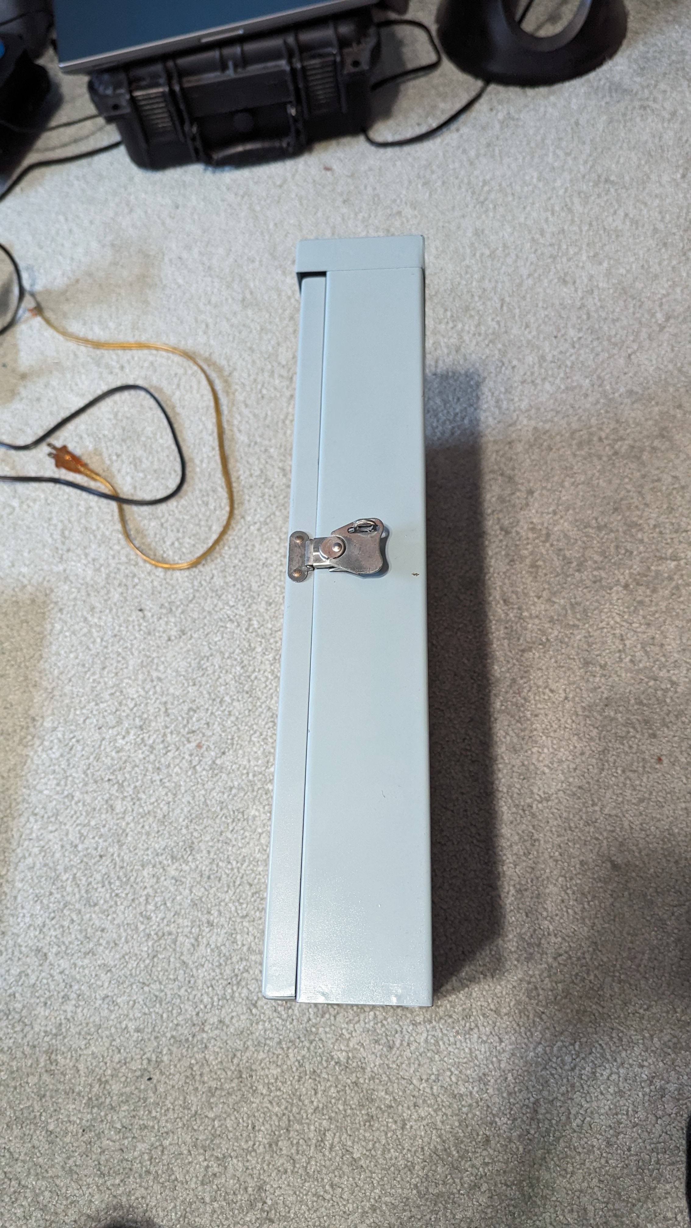
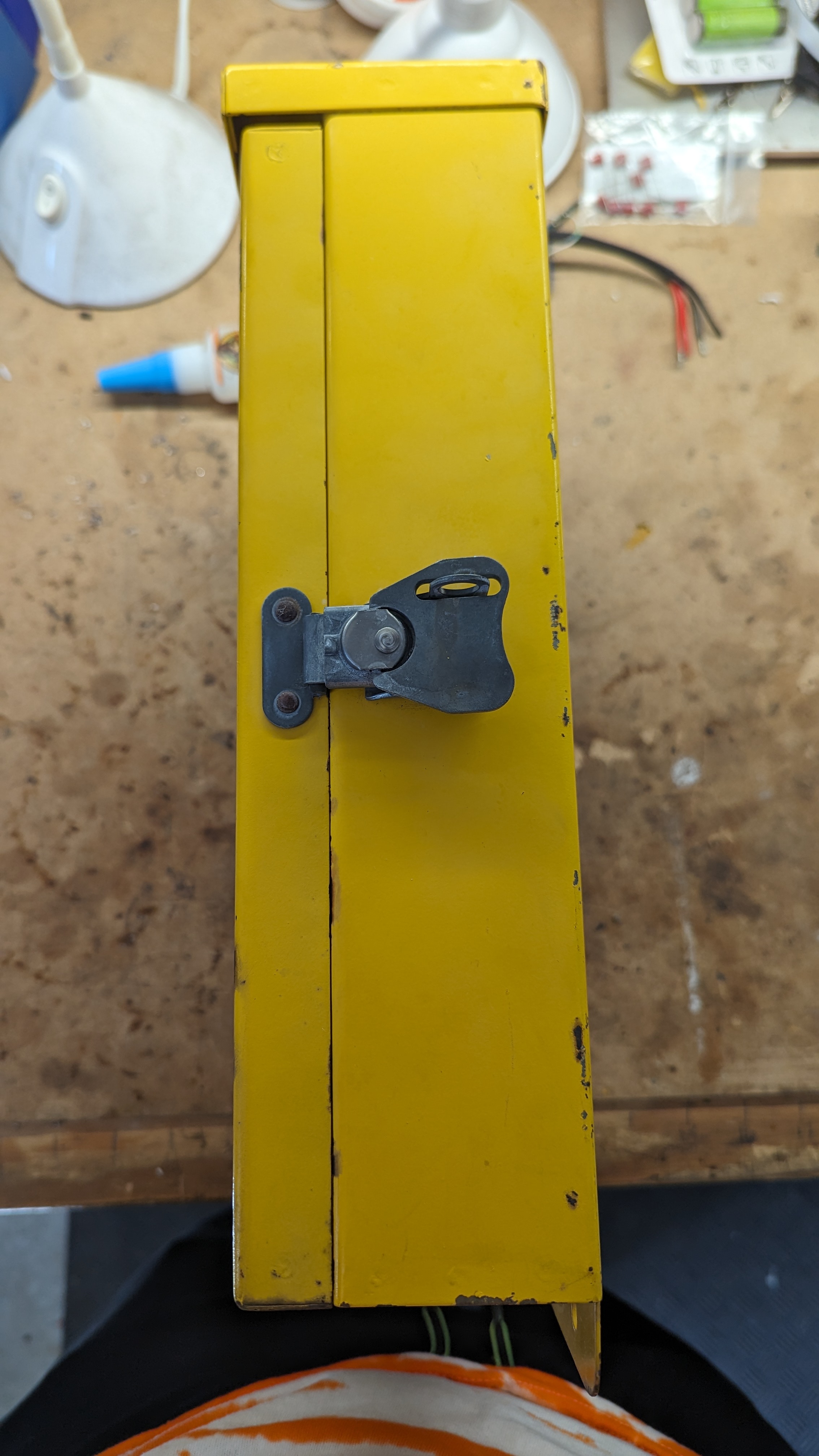
| 23:10, 15 April 2024 | Cdf latch side.jpg (file) |  |
1.2 MB | Side of the enclosure with latch. First flips out, then rotate the wing to loosen the clamp. | 1 |