Blink SyncModule 2: Difference between revisions
Added detailed picture and description of one unknown IC. |
mNo edit summary |
||
| (12 intermediate revisions by 3 users not shown) | |||
| Line 15: | Line 15: | ||
==Main components== | ==Main components== | ||
===Microcontroller=== | The Blink Sync Module 2 has 2 documented board types, they can easily be identified by the microprocessor being mounted on the bottom or top of the PCB, if the chip is on the bottom board rev = A0 Blink board. | ||
NXP MCIMX6Z0DVM09AB<ref name="NXP MCIMX6Z0DVM09AB"> | |||
===Amazon Board=== | |||
====Microcontroller==== | |||
NXP MCIMX6Z0DVM09AB<ref name="NXP MCIMX6Z0DVM09AB">https://www.nxp.com/part/MCIMX6Z0DVM09AB#/</ref> | |||
*[[ARM]] [[Cortex-A7]] running Linux | *[[ARM]] [[Cortex-A7]] running Linux | ||
| Line 25: | Line 29: | ||
*Has Arm TrustZone | *Has Arm TrustZone | ||
===Wifi/Bluetooth Module=== | ====Wifi/Bluetooth Module==== | ||
[[NXP]] 88W8987-NYE2<ref name="NXP 88W8987-NYE2"> | [[NXP]] 88W8987-NYE2<ref name="NXP 88W8987-NYE2">https://www.nxp.com/products/wireless-connectivity/wi-fi-plus-bluetooth-plus-802-15-4/2-4-5-ghz-dual-band-1x1-wi-fi-5-802-11ac-plus-bluetooth-5-2-solution:88W8987</ref> | ||
*2.4/5Ghz Wifi | *2.4/5Ghz Wifi | ||
*Bluetooth 5.2 (BLE also) | *Bluetooth 5.2 (BLE also) | ||
===Serial flash=== | ====Serial flash==== | ||
[[Winbond]] 25Q256JVEQ<ref name="Winbond 25Q256JVEQ"> | [[Winbond]] 25Q256JVEQ<ref name="Winbond 25Q256JVEQ">https://www.winbond.com/hq/product/code-storage-flash-memory/serial-nor-flash/?__locale=en&partNo=W25Q256JV</ref> | ||
*256M-bit | *256M-bit | ||
*Dual/Quad SPI XIP (133MHz SPI) | *Dual/Quad SPI XIP (133MHz SPI) | ||
===RAM=== | ====RAM==== | ||
[[ISSI]] IS43TR16640BL<ref name="ISSI IS43TR16640BL"> | [[ISSI]] IS43TR16640BL<ref name="ISSI IS43TR16640BL">https://www.issi.com/WW/pdf/43-46TR16640B-81280BL.pdf</ref> | ||
*1GB SDRAM | *1GB SDRAM | ||
*16bit DDR3 | *16bit DDR3 | ||
====Sub-GHz "EZRadio" Transceiver==== | |||
Markings: 455A CQRX 220 | |||
Silicon Labs Si4455<ref name=":0">https://www.silabs.com/documents/public/data-sheets/Si4455.pdf</ref> | |||
*Frequency of 283–960 MHz | |||
*–116 dBm Sensitivity | |||
*Modulation: | |||
**(G)FSK | |||
**OOK | |||
*+13 dBm Max output power | |||
*50 nA Standby Current | |||
*500 kbps Max Data Rate | |||
*1.8 to 3.6 VDC <br /> | |||
===Rev A0 Blink Board=== | |||
====Microcontroller==== | |||
[[Atheros]] AR9331 rev 1 (MIPS 24Kc @ 400MHz) - [https://github.com/luekker/blink-sync-module-2/blob/main/docs/Atheros%20-%20AR9331.pdf] | |||
====Wifi Module==== | |||
Onboard [[Atheros]] AR9331 | |||
====Serial flash==== | |||
[[Winbond]] 25Q64 | |||
====RAM==== | |||
[[ISSI]] IS43TR16640BL<ref name="ISSI IS43TR16640BL" /> | |||
*64mb DDR2 16 bit | |||
====Sub-GHz "EZRadio" Transceiver==== | |||
Markings: 455A CQRX 220 | |||
Silicon Labs Si4455<ref name=":0" /> | |||
*Frequency of 283–960 MHz | |||
*–116 dBm Sensitivity | |||
*Modulation: | |||
**(G)FSK | |||
**OOK | |||
*+13 dBm Max output power | |||
*50 nA Standby Current | |||
*500 kbps Max Data Rate | |||
*1.8 to 3.6 VDC | |||
==Teardown pictures== | ==Teardown pictures== | ||
====Amazon Board==== | |||
<gallery> | <gallery> | ||
File:Blink syncmodule2 photo1.jpg|Front face of the BSM2 | File:Blink syncmodule2 photo1.jpg|Front face of the BSM2 | ||
| Line 55: | Line 107: | ||
File:Photo10.jpg|MCU closeup | File:Photo10.jpg|MCU closeup | ||
File:Photo11.jpg|SRAM closeup | File:Photo11.jpg|SRAM closeup | ||
File: | File:Unknown ic.png|Si4455 | ||
File:Photo12.jpg|Wifi/BT module closeup | File:Photo12.jpg|Wifi/BT module closeup | ||
File:Bottom layer zoom.jpg | |||
File:Sync module 2 top layer zoom.jpg | |||
</gallery><br /> | |||
====Rev A0 - Blink Board==== | |||
<gallery> | |||
File:Blink-sync-module-2-shell.jpg|Outer shell | |||
File:Blink Sync Module 2 - rev a0 - Pins.png|Labelled Pins, TM1 = RX, TM2 = TX, TM3 = GND | |||
File:Blink sync module 2 PCB (top) - rev a0.jpg|Top face | |||
File:Blink Sync Module 2 PCB (bottom) - Rev A0.jpg|Bottom face | |||
</gallery> | </gallery> | ||
==Serial Communications== | |||
It is possible to read the boot of the device by connecting to the indicated pin. | |||
Baud rate is 115200. | |||
====Amazon Board==== | |||
[[File:Txpin.png|none|frame]]<br /> | |||
====Rev A0 - Blink Board==== | |||
TM2 for reading UART | |||
[[File:Blink Sync Module 2 - rev a0 - Pins.png|none|thumb]]<br /> | |||
==References== | |||
<references /> | <references /> | ||
Latest revision as of 00:31, 11 February 2026

What is it?
Home appliance to control other Amazon Blink devices.
According to the manufacturer: "The Sync Module is a hub that plugs into an electrical outlet to relay commands and network details to devices in the system it manages. The Sync Module 2 requires a power outlet and is connected to your always-on Wi-Fi network to handle activity for up to ten Blink devices. This extends camera battery life, saves clips without a subscription, improves convenience for scheduling, and arms a group of devices at once."[1]
What can it do?
- Control Blink devices (cameras, doorbells, etc) from the Blink mobile app
- Connect up to 10 of any Blink Outdoor 4, Wired Floodlight, Outdoor and Indoor (all models), XT2, XT, Video Doorbell*, and Mini* cameras.
- Support local video storage for up to 10 Blink cameras.
- Record and store motion clips when you insert a USB flash drive (up to 256 GB).
Main components
The Blink Sync Module 2 has 2 documented board types, they can easily be identified by the microprocessor being mounted on the bottom or top of the PCB, if the chip is on the bottom board rev = A0 Blink board.
Amazon Board
Microcontroller
NXP MCIMX6Z0DVM09AB[2]
- ARM Cortex-A7 running Linux
- 900MHz
- SRAM: 128kB
- SPI/UART/I2C
- 96KB bootrom, 128KB internal RAM
- Has Arm TrustZone
Wifi/Bluetooth Module
- 2.4/5Ghz Wifi
- Bluetooth 5.2 (BLE also)
Serial flash
- 256M-bit
- Dual/Quad SPI XIP (133MHz SPI)
RAM
- 1GB SDRAM
- 16bit DDR3
Sub-GHz "EZRadio" Transceiver
Markings: 455A CQRX 220
Silicon Labs Si4455[6]
- Frequency of 283–960 MHz
- –116 dBm Sensitivity
- Modulation:
- (G)FSK
- OOK
- +13 dBm Max output power
- 50 nA Standby Current
- 500 kbps Max Data Rate
- 1.8 to 3.6 VDC
Rev A0 Blink Board
Microcontroller
Atheros AR9331 rev 1 (MIPS 24Kc @ 400MHz) - [1]
Wifi Module
Onboard Atheros AR9331
Serial flash
Winbond 25Q64
RAM
- 64mb DDR2 16 bit
Sub-GHz "EZRadio" Transceiver
Markings: 455A CQRX 220
Silicon Labs Si4455[6]
- Frequency of 283–960 MHz
- –116 dBm Sensitivity
- Modulation:
- (G)FSK
- OOK
- +13 dBm Max output power
- 50 nA Standby Current
- 500 kbps Max Data Rate
- 1.8 to 3.6 VDC
Teardown pictures
Amazon Board
-
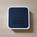 Front face of the BSM2
 -
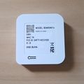 Back face of the BSM2
 -
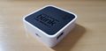 Top view
 -
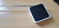 To take off the top part just use a spudger, guitar pic, etc. No glue or screws to take the top cover off.
 -
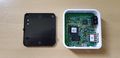 PCB view (top)
 -
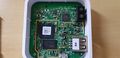 PCB view (top) closeup
 -
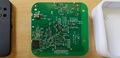 PCB view (bottom)
 -
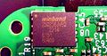 Serial Flash closeup
 -
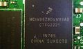 MCU closeup
 -
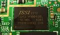 SRAM closeup
 -
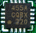 Si4455
 -
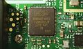 Wifi/BT module closeup
 -
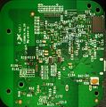
-
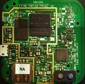


Rev A0 - Blink Board
-
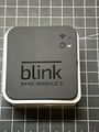 Outer shell
 -
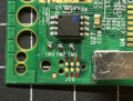 Labelled Pins, TM1 = RX, TM2 = TX, TM3 = GND
 -
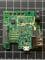 Top face
 -
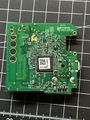 Bottom face

_-_rev_a0.jpg)
_-_Rev_A0.jpg)
Serial Communications
It is possible to read the boot of the device by connecting to the indicated pin.
Baud rate is 115200.
Amazon Board

Rev A0 - Blink Board
TM2 for reading UART

References
- ↑ [ https://support.blinkforhome.com/en_US/faq-sm/sync-module-2-faqs]
- ↑ https://www.nxp.com/part/MCIMX6Z0DVM09AB#/
- ↑ https://www.nxp.com/products/wireless-connectivity/wi-fi-plus-bluetooth-plus-802-15-4/2-4-5-ghz-dual-band-1x1-wi-fi-5-802-11ac-plus-bluetooth-5-2-solution:88W8987
- ↑ https://www.winbond.com/hq/product/code-storage-flash-memory/serial-nor-flash/?__locale=en&partNo=W25Q256JV
- ↑ 5.0 5.1 https://www.issi.com/WW/pdf/43-46TR16640B-81280BL.pdf
- ↑ 6.0 6.1 https://www.silabs.com/documents/public/data-sheets/Si4455.pdf