Roland DIF-AT: Difference between revisions
Created page with "PCB photos, Pinouts, Pin header, Device operation, Connections between subsystems. Notes on firmware structure, Machine language monitor program, DFU, firmware extraction, fir..." |
m continued adding info to the page |
||
| Line 1: | Line 1: | ||
[Page under construction - as yet incomplete] | |||
PCB photos, Pinouts, Pin header, Device operation, Connections between subsystems. Notes on firmware structure, Machine language monitor program, DFU, firmware extraction, firmware update script (python) | PCB photos, Pinouts, Pin header, Device operation, Connections between subsystems. Notes on firmware structure, Machine language monitor program, DFU, firmware extraction, firmware update script (python) | ||
| Line 4: | Line 7: | ||
[[File:DIFAT 24.jpg|thumb|rolands publicity image (still online)]] | [[File:DIFAT 24.jpg|thumb|rolands publicity image (still online)]] | ||
=== Brief outline === | ===Brief outline -=== | ||
I bought this device to repair. They are rare, and interesting. It would not respond any longer or be recognised by host hardware. | I bought this device to repair. They are rare, and interesting. It would not respond any longer or be recognised by host hardware. | ||
| Line 13: | Line 16: | ||
Given the device was already non-responsive (and now damaged) - | Given the device was already non-responsive (and now damaged) - | ||
Goals- | === Goals- === | ||
=== PCB Photos === | #De-solder NOR Flash and read firmware. | ||
#Determine potential corruption of firmware. | |||
#Re-flash firmware onto new NOR flash (if good). | |||
#Determine operation / potential corruption of Xilinx CPLD and/or Alesis OTP? IC - read contents if possible. | |||
#Analyse firmware for anything interesting. | |||
#Determine and examine / analyse hardware architecture. | |||
#Repair traces, replace ICs. Test. | |||
#Collate information, share research and findings. | |||
===PCB Photos -=== | |||
<gallery> | <gallery> | ||
DIF-AT MAIN.JPG|Main board | File:DIF-AT MAIN.JPG|Main board | ||
H8 3005 CPU.JPG|Cpu (not mcu!) | File:H8 3005 CPU.JPG|Cpu (not mcu!) | ||
Main Board Side On.JPG|Main board, alt | File:Main Board Side On.JPG|Main board, alt | ||
SRAM + NOR FLASH.JPG|SRAM + NOR Flash (512kb) | File:SRAM + NOR FLASH.JPG|SRAM + NOR Flash (512kb) | ||
ALESIS OTP CPLD.JPG|Custom Alesis chip OTP? | File:ALESIS OTP CPLD.JPG|Custom Alesis chip OTP? | ||
TDIF-BOARD.JPG|TDIF daughter board | File:TDIF-BOARD.JPG|TDIF daughter board | ||
</gallery> | </gallery> | ||
<br /> | |||
== Device Overview == | |||
This is a complex device with a 16 bit CPU, Xilinx 95xx CPLD, Custom Alesis chip (Gate array, PAL, GAL, OTP CPLD?) SRAM, NOR flash 512kb, logic and switching for bus arbitration. BREQ Bus request is a very involved circuit. Also CE# Chip Enable NOR Flash is connected through a complicated muxing circuit. | |||
It has 2 buttons on the PCB: 1 - RESET, reset circuit and IC 2 - Launch monitor diagnostic mode. 50 pin header provides easy access to most address lines and relevant (to operation) CPU/RAM/Flash lines. This will be convenient to run a logic capture during boot and operation later. | |||
I mapped out the 50 pin connector - | |||
<br /> | |||
== Extract Firmware == | |||
In the past I've done firmware upgrades on synths, so I used a TL48 programmer with a 48pin TTSOP | |||
[more is coming, I'll continue editing this page in the coming days] | [more is coming, I'll continue editing this page in the coming days] | ||
Revision as of 08:53, 27 April 2026
[Page under construction - as yet incomplete]
PCB photos, Pinouts, Pin header, Device operation, Connections between subsystems. Notes on firmware structure, Machine language monitor program, DFU, firmware extraction, firmware update script (python)

Brief outline -
I bought this device to repair. They are rare, and interesting. It would not respond any longer or be recognised by host hardware. (it runs in conjunction with host digital mixer / host music production device, translating digital audio formats in real time)
I damaged a lot of traces on the device and gave up on it. However, I learned how to micro-solder and became inspired to continue the repair with reverse engineering techniques.
Given the device was already non-responsive (and now damaged) -
Goals-
- De-solder NOR Flash and read firmware.
- Determine potential corruption of firmware.
- Re-flash firmware onto new NOR flash (if good).
- Determine operation / potential corruption of Xilinx CPLD and/or Alesis OTP? IC - read contents if possible.
- Analyse firmware for anything interesting.
- Determine and examine / analyse hardware architecture.
- Repair traces, replace ICs. Test.
- Collate information, share research and findings.
PCB Photos -
-
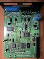 Main board
 -
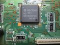 Cpu (not mcu!)
 -
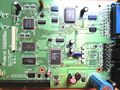 Main board, alt
 -
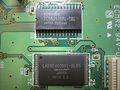 SRAM + NOR Flash (512kb)
 -
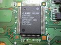 Custom Alesis chip OTP?
 -
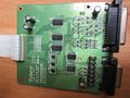 TDIF daughter board


Device Overview
This is a complex device with a 16 bit CPU, Xilinx 95xx CPLD, Custom Alesis chip (Gate array, PAL, GAL, OTP CPLD?) SRAM, NOR flash 512kb, logic and switching for bus arbitration. BREQ Bus request is a very involved circuit. Also CE# Chip Enable NOR Flash is connected through a complicated muxing circuit.
It has 2 buttons on the PCB: 1 - RESET, reset circuit and IC 2 - Launch monitor diagnostic mode. 50 pin header provides easy access to most address lines and relevant (to operation) CPU/RAM/Flash lines. This will be convenient to run a logic capture during boot and operation later.
I mapped out the 50 pin connector -
Extract Firmware
In the past I've done firmware upgrades on synths, so I used a TL48 programmer with a 48pin TTSOP
[more is coming, I'll continue editing this page in the coming days]