Roland DIF-AT
[Page under construction - as yet incomplete]
PCB photos, Pinouts, Pin header, Device operation, Connections between subsystems. Notes on firmware structure, Machine language monitor program, DFU, firmware extraction, firmware update script (python)

Brief outline -
I bought this device to repair. They are rare, and interesting. It would not respond any longer or be recognised by host hardware. (it runs in conjunction with host digital mixer / host music production device, translating digital audio formats in real time)
I damaged a lot of traces on the device and gave up on it. However, I learned how to micro-solder and became inspired to continue the repair with reverse engineering techniques. This is my first reverse engineering project, though I have worked on modding and repairing before.
Given the device was already non-responsive (and now damaged) -
Goals-
- De-solder NOR Flash and read firmware.
- Determine potential corruption of firmware.
- Re-flash firmware onto new NOR flash (if good).
- Determine operation / potential corruption of Xilinx CPLD and/or Alesis OTP? IC - read contents if possible.
- Analyse firmware for anything interesting.
- Determine and examine / analyse hardware architecture.
- Repair traces, replace ICs. Test.
- Collate information, share research and findings.
PCB Photos -
-
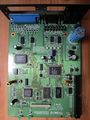 Main board
 -
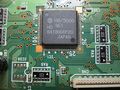 Cpu (not mcu!)
 -
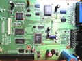 Main board, alt
 -
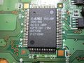
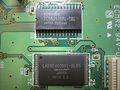 SRAM + NOR Flash (512kb)
 -
 Custom Alesis chip OTP?
 -
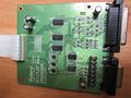 TDIF daughter board


Device Overview
This is a complex device with a 16 bit CPU, Xilinx 95xx CPLD, Custom Alesis chip (Gate array, PAL, GAL, OTP CPLD?) SRAM, NOR flash 512kb, logic and switching for bus arbitration. BREQ Bus request is a very involved circuit. Also CE# Chip Enable NOR Flash is connected through a complicated muxing circuit.
The Device is quite old school, this was built for the early generation of ADAT/TDIF machines, still using physical tape. Though tape is not necessary for operation, the sync requirements of locking digital audio, using analogue tape, add a lot of complexity.
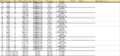
It has 2 buttons on the PCB: 1 - RESET, reset circuit and IC 2 - Launch monitor diagnostic mode. A 50 pin header provides easy access to most address lines and relevant (to operation) CPU/RAM/Flash lines. This will be convenient to run a logic capture during boot and operation later.
I beeped out the 50 pin connector - Many pins have multiple connections. Happily; the vias were not tented - this was a long endeavour even with
continuity through the vias : )
-
 header pins 1 - 16
 -
 header pins 16 - 24
 -
 header pins 15 to 38
 -
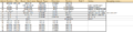 header pins 38 to 50
 -
 general notes about CPU SRAM, inferred operation


Extract Firmware
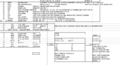
I used a TL48 programmer with a 48pin TTSOP to read the firmware contents -
Below in the image are the settings needed for a good read. The NOR flash is 16 bit wide, but the CPU is reading it in 8 bit mode (8 bit mode pin is tied low). SHARP LH28F400BVE Parallel NOR Flash 512kb. The chip is from the late 1990s as the device is also, turn of the century 2000s.
Although the strings are legible here, it is because the T48 is re-arranging the byte order automatically. The byte order must be swapped (little endian) in order to disassemble the firmware. I found this out after nonsensical strings were seen, without swapping byte order. I tried some 8 bit reads, but this garbled the strings in the T48. It was clear 16 bit wide was correct, but then byte order needed changing. I used a python script for that.
The strings are very interesting indeed, not just a standard version string - they are command strings. As this device has no screen, a low level diagnostic routine is inferred from their discovery. Looking closely at the last string or two, I was worried that it might be corrupted as there are some missing letters in the string - (ADAT Sync port di onnected and Dectected rather than Detected).
