LMS-6 Radiosonde
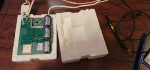
The LMS-6 Radiosonde is a balloon-launched radiosonde manufactured by Lockheed-Martin Sippican, and used for meteorological sounding.
Contents
- 1 Overview
- 2 Specs
- 3 Photos
- 4 Audio Samples
- 5 Disassembly
- 6 Reassembly
- 7 Powering the radiosonde in the lab
- 8 Connectors
- 9 Components
- 10 GPS Subsystem
- 11 CC1050 Subsystem
- 12 Test Points
- 13 Circuits
- 14 Original Firmware
- 15 Modifications
- 16 Instruction Timing Tables
- 17 Ideas for doing AFSK modulation on 70CM with CC1050 and ST7
- 18 ST7 Programming
- 19 Reference
Overview
There are two models of the LMS-6, a 403MHz model and a 1680MHz model. This article will cover the 403MHz model unless specified.
Specs
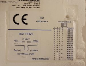
- 16 Fixed transmit carrier frequencies (MHz): 400.250, 400.625, 401.000, 401.375, 401.750, 402.125, 402.500, 402.875, 403.250, 403.625, 404.000, 404.375, 404.750, 405.125, 405.500, 405.875
- Frequency tolerance +/-30ppm
- Mean TX Power 70.8mW (18.5dBm)
- Emission Designator 16K8F1D
- FSK with a maximum modulating frequency of 4.8 kHz
- Emission 3dB BW +/-5.0 kHz
- Emission 20dB BW +/-12.7 kHz
- Omnidirectional antenna
- Main beam gain 2dBi
- Horizontal Beamwidth 360 degrees
- Vertical Beamwidth +84 degrees
Source: https://apps.fcc.gov/els/GetAtt.html?id=121623&x=.
Photos
Audio Samples
The following samples were taken from both frequency versions at a close distance using a HackRF SDR.
| Frequency | Audio file |
|---|---|
| 400 MHz | |
| 1680 MHz |
Disassembly
This is a minimally-destructive disassembly method that will allow the payload to be held back together if you wish to reuse the payload for another weather balloon flight.
- Cut the zip tie holding the plastic strap to the balloon/parachute tether rope.
- Examine rope, parachute and parachute rigging lines for viability. Neatly organize the flight rigging if usable. Discard if not viable for reuse.
- Peel open the battery/power cover from the bottom of the radiosonde and ensure that all 3 connectors are loose and not connected to one another.
- Remove the plastic pins from either side of the radiosonde.
- Peel away the paper wrapper starting with the corner near the external sensors
- Tear the plastic strap off. It's held on mostly with a few staples into the styrofoam
- Using a sharp utility razor, cut the bottom half of the shell off, carefully. The styrofoam is about 0.6 inch (15mm) thick on both the sides and bottom, so making a long cut all the way around the sides of the radiosonde, about 0.75" from the bottom edge, and not much deeper than 0.6" is recommended. You can use the exit of the weather sensors as a guide. DO NOT fully separate the radiosonde styrofoam shell yet.
- Cut the tape holding the antenna into its dipole shape. Completely remove the tape and straighten the antenna wires.
- Peel open the battery terminal access panel on the bottom again. Using a pair of tweezers, remove the small styrofoam block keeping the power wires restrained.
- Push the battery wires through the hole as you peel apart the styrofoam shell.
- The shell is glued together from the factory. Some of this glue will hold wires to the styrofoam shell. Carefully peel the sensor wires away from the foam and carefully pull the antenna wire (straightened in step 8) through the hole in the bottom of the shell.
- The board should be completely separated from the two styrofoam shell halves. Set aside shell, plastic strap, plastic pins and paper wrap for possible re-use later.
- Remove (3) Lithium CR-123A cells from the battery holders and discard of them safely.
Reassembly
- Place fresh lithium CR-123A cells into the battery holders. Use of rechargeable cells is not recommended for high-altitude flight.
- Pass antenna wire through bottom part of shell.
- Pass all 3 power wires through the bottom part of shell and into the power lead compartment.
- Make sure radiosonde circuit board is properly aligned and seated into the bottom half of the shell.
- Replace small styrofoam brick to hold power wires into the compartment. Do not connect any power wires together yet.
- Route the antenna flat against the bottom of the shell.
- Place upper half of shell onto lower half of shell, ensuring that the weather sensors are able to exit the side of the shell where they originally did.
- Affix the two halves of the radiosonde shell together. Long, sturdy zip-ties (one around where the plastic strap goes, another one or two perpendicular to it over the top and bottom) would likely work well and remain intact while exposed to the potentially harsh and cold elements at high altitudes. Alternative closures could be twine (if properly tied) or hot glue, which seems to be what is used to seal the radiosonde at the factory. Glues and cements may make further re-use problematic if you intend to recover and fly the radiosonde multiple times.
- Place the plastic strap around the radiosonde as originally equipped. You can likely push the staples back into the styrofoam if they're left intact.
- Optionally, re-attach the paper wrapper to the payload, or feel free to attach your own wrapper or identification.
- Replace the plastic pins that hold the plastic strap to the radiosonde payload.
- Ensure all sensors and antenna are extended and oriented properly. Be sure to bend the antenna into a dipole orientation similar to how it shipped (about 5.75" of the shorter lead folded back and held about 0.5" away from the twin-lead coming from the radiosonde)
- Optionally, use a loop of tape to ensure the dipole antenna remains positioned appropriately, similar to how the antenna was originally rigged.
- Attach radiosonde strap to flight rigging (rope/parachute/balloon or your choice of drone, kite, etc)
- Remember to connect the red and white wires, and do a pre-flight telemetry verification immediately before launch.
Powering the radiosonde in the lab
The OEM battery bank consists of three (3) CR-123A cells in series at 3.0VDC each, for a total of 9VDC. These cells are relatively expensive and only power the unit for 6-7 hours at a time. Internal battery power is enabled by connecting the white and red power wires together inside the compartment on the bottom of the radiosonde.
The unit can be powered on the bench by providing 9VDC to the red power wire and connecting the black wire to power supply ground. Do not exceed 10VDC. Lithium-Ion rechargeable RCR-123A cells can also be used for testing. These cells will not likely last the duration of a high-altitude balloon flight due to both limited power capacity and cold temperatures at altitude.
Connectors
There are four sensor connectors (SENSN) used for sensor input by the radiosonde. SENS1 is not populated on the 403MHz units. SENS2-4 have leads connected to them, and the sensors are connected to the other end of the leads, outside of the radiosonde housing. Only SENS1 appears to have spacing for a connector; the others have arbitrary lead spacing.
| Pin | Characteristics |
|---|---|
| 1 | +5V (5.47 measured) - From U25 |
| 2 | GND |
| 3 | U3 Pin 37 (PA7, High Sink/20mA) |
| 4 | 1 Hz - U14 (Analog MUX) Pin 9 (S2) |
| 5 | 1 Hz - U14 Pin 11 (S1) |
| 6 | 1 Hz - U14 Pin 11 (S0) |
| 7 | Pulldown via R41 (47k) to GND |
Public information shows this header may be used for adding additional analog sensors to the radiosonde.
| Pin | Connection |
|---|---|
| 1 | Sensor pin 1 |
| 2 | Sensor pin 2 |
0.3" spacing. Both lead wires have ferrite beads immediately before connecting to the board.
| Pin | Connection |
|---|---|
| 1 | Sensor pin 1 |
| 2 | Sensor pin 2 |
0.5" spacing.
| Pin | Connection |
|---|---|
| 1 | Sensor pin 1 |
| 2 | Sensor pin 2 |
0.3" spacing. Fine gauge insulated wire run along SENS3 wire and loomed in white heat-shrink tubing.
| Pin Number | Function | Notes / Observations | Pin Number | Function | Notes / Observations |
|---|---|---|---|---|---|
| 1 | Vdd | U3 - Vdd
U15 - Pin 4 |
2 | Vdd | U3 - Vdd
U15 - Pin 4 |
| 3 | U3 - Pin29 / PC6 / SCK / ICCCLK
TP33 U21 - Pin21 / PCLK |
4 | U3 - Pin38/Vpp/ICCSEL | Programmer probably has a 5->12v charge pump for this.
Do not apply 12v willy-nilly, will blow chip. | |
| 5 | U3 - Pin39/RESET | 6 | U3 - Pin27 / PC4 / MISO / ICCDATA | ||
| 7 | Vdd | U3 - Vdd
U15 - Pin 4 |
8 | Vdd | U3 - Vdd
U15 - Pin 4 |
| 9 | GND | 10 | GND | ||
| 11 | J5 - Pin 2 | 12 | U21 - Pin 20 - DCLK | 3.3v - 4800Hz square wave, clocks the serial data
This is probably not directly connected to ST7 PortF.4 which is 5V. | |
| 13 | SW1.4 | U3 - Pin10/AIN3/PD3
51K resistor to ground |
14 | ||
| 15 | GND | 16 | GND | ||
| 17 | SW1.2 | U3 - Pin8/AIN1/PD1
51K resistor to ground |
18 | SW1.1 | U3 - Pin7/AIN0/PD0
51K resistor to ground |
| 19 | GND | 20 | GND | ||
| 21 | 47k pullup
U3 - Pin19 |
Appears to be some sort of test-mode select, checked before GPIO initialization. | 22 | ||
| 23 | GPS TX Data (38400 BPS)
U3 - Pin1/RDI |
Data bursts | 24 | +5VDC ? | |
| 25 | 26 | GPS RX Data (38400 BPS)
Maybe not connected to U3? |
Data bursts | ||
| 27 | 28 | ||||
| 29 | 30 | U22.3 | U22 Pin 3 3V3 Enable (Active Low)
Connected to R38 pull-down Connected to JP27 | ||
| 31 | BATT POS | 32 | J5 - Pin 3 | ||
| 33 | GND | 34 | GND | ||
| 35 | 36 | SW1.3 | U3 - Pin9/AIN2/PD2
51K resistor to ground | ||
| 37 | 38 | U3 - Pin18 / OCMP1_A / AIN10 / PF4 | Square wave data bursts, 0.2msec per bit | ||
| 39 | RED WIRE | 40 | Battery voltage | Around 9VDC measured, 3x3V batteries |
Compatible connector: TE Connectivity AMP Connectors 5-5530843-4 such as Digi-Key A31723-ND[1]
| Pin | Wire Color | Use |
|---|---|---|
| 1 | Black | Ground |
| 2 | White | Battery +9 |
| 3 | Red | +9 VDC In |
| 4 | NC | Unknown - goes to
unpopulated CR1 |
J4 - NC - earphone jack? uses SENS3 leads
| Pin | Description |
|---|---|
| 1 | GND |
| 2 | To (?, maybe nothing); to +5 via R7 (47k) (And Card-Edge pin 11) |
| 3 | To U3.11 (AIN4/PD4) via R47 (100); to +5 via R7 (47k) (And Card-Edge pin 32) |
| 4 | GND |
| Pin | Description | Pin | Description |
|---|---|---|---|
| 1 | +5VDC - All from U9 | 2 | U14 (Analog MUX) Pin 13 (A0) - 3V rounded square pulses, 2x per second, 2 different periods avg ~75msec? |
| 3 | +5VDC | 4 | U14 Pin 14 (A1) - 5V, 0.1msec pulse once per second |
| 5 | +5VDC | 6 | U14 Pin 15 (A2) - 5V, 0.1msec pulse once per second |
| 7 | +5VDC | 8 | U14 Pin 12 (A3) - 3V, 250msec pulse once per second |
SP1 connects to four channels of U14, an 8-channel analog MUX. Pin 2 also connects to R111, non-populated, which would provide a pull-up to +5 at Pin 1.
Components
The following is a catalog of active components. Designators italicized still need positive identification; bold have been positively identified. Markings listed where known to help in identification. List additional markings when they differ.
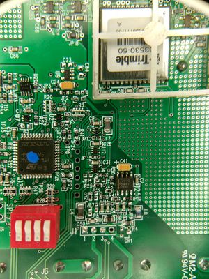
U1 - GPS - Trimble 63530-50 - 12-channel GPS, 2x serial ports, 2.7-3.3VDC, SBAS, flash almanac/ephemeris/location storage. (The -50 variant is probably a custom variant, and exact capabilities are unknown.)
- This chip defaults to TSIP on the 38400 baud port, which is a binary protocol, and has been captured on this PCB.
- TSIP Protocol Documentation
U2 - (Marked G4/905)
U3 - ST72F324J6T6 - 32K Flash, 1K RAM, 5VDC, 10-bit ADC (16 inputs, muxed), 4x Timer, SPI, SCI, 32-bits total I/O
- 72F324J6T6 - ST72324 - Main Microcontroller, ST7 series Datasheet
- ST7 Family Programming Manual ( For coders)
- ST7 Flash Programming Quick Reference Guide
- ST7 Family Flash Programming Reference Manual
- ST7 Family ICC Protocol Reference Manual
- With a buffered 16MHz clock provided by Y3/U12, possible CPU speeds are 8MHz(/1), 4MHz(/2), 2MHz(/4), 1MHz(/8) depending on MCC configuration.
- Instruction timings are in the 'ST7 Family Programming Manual'
U4 - (Marked Z252)
U5, U6 - LP2985 - LDO - 2.8V?
U7 - (Marked G4/905)
U8 - (Marked G4/905)
U9 - (Marked F50)
U10 - (Did not locate, maybe not placed?)
U11 - (Marked 73RW, SOT-89 or similar) - Pre-amp for GPS ant? In GPS section can.
U12 - (Marked G5/849) - looks like a clock buffer between Y3 and U3
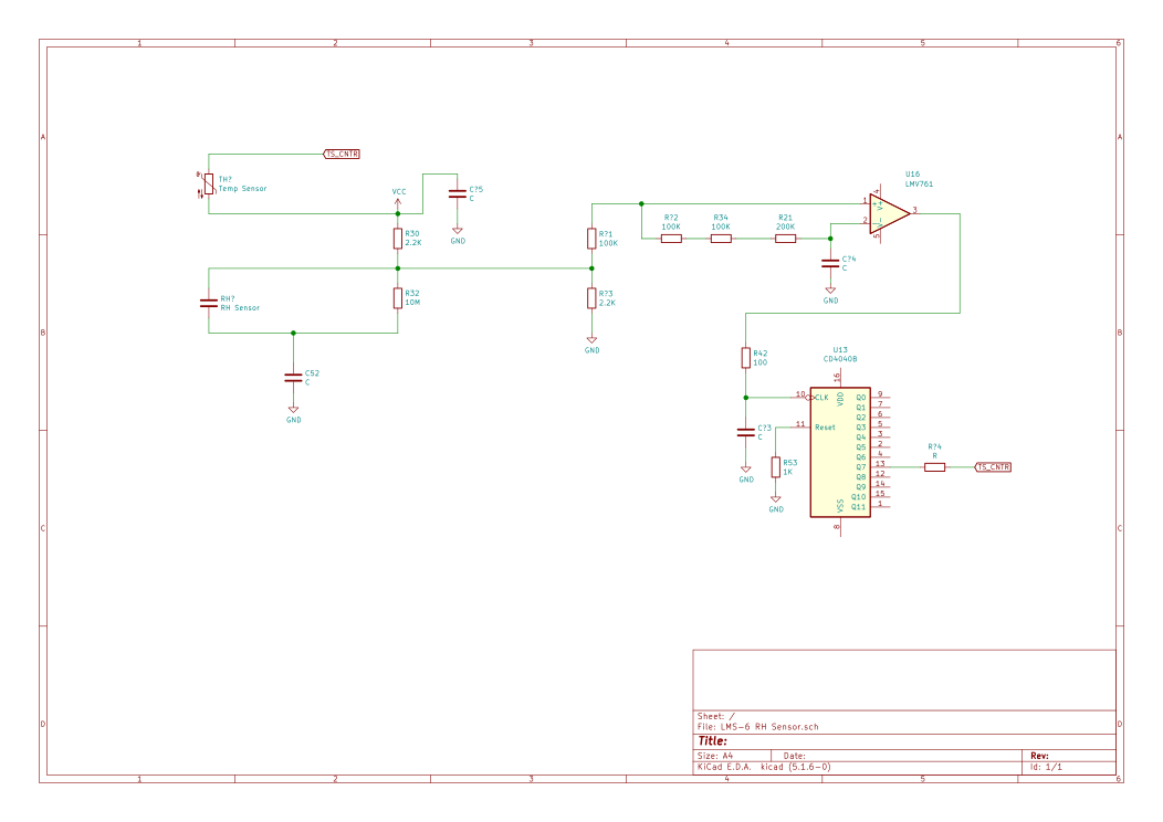
U13 - CD4040BPW - 12-stage Ripple-Carry Binary Counter/Divider [IC Footnotes 1]
U14 - CD74HC4051PWR - High-Speed CMOS Logic Analog Mux/Demux - 8:1
U15 - TI LMC555CMM Family [IC Footnotes 2]
U16 - LMV761MF - Low Voltage Precision Comparator w/ Push-Pull Output [IC Footnotes 3]
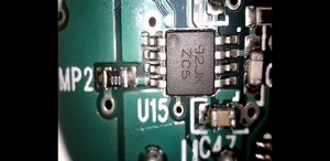
U17 - (Marked Z252) - 3v(blue) -> 5v(yellow) level translator *insert picture U17 here*
U18 - (Did not locate, maybe not placed?)
U19 - (Did not locate, maybe not placed?)
U20 - Toshiba TC7WH157FU
U21 - CC1050 (back) - Low Power Transmitter - 300MHz-1000MHz, variable power, FSK
U22 - TPS79133DBUR - 3.3V LDO - for U21
Unot_marked (23/24?) - (Marked W6K/W76) - RF Amp, similar to SKY65013-70LF (No designator; under TX can to bottom-right of U21.)
U25 - TPS7201Q - Adj. 1.2-9.75V LDO - (Designator silkscreen is hard to read; 8-SOIC on bottom-right)
Y3 - 16MHz crystal
| U15 Pin | Function | Observations/Notes |
|---|---|---|
| 1 | GND | |
| 2 | 5VDC | |
| 3 | Trigger | Rounded square wave (maybe sawtooth) alternating between 2msec and 4msec, resting at +3VDC between bursts |
| 4 | Discharge | Rounded square wave alternating between 3msec and 5msec, short periods of 0v, resting at +3VDC between bursts |
| 5 | Output | Data. Square wave. 5V space, 0v mark? Pulses around 250msec per bit. Perhaps this is a capacitance or resistance to frequency converter. |
| 6 | Threshold | More rounded square wave bursts |
| 7 | Reset | |
| 8 | Control |
Sens 4 - Capacitive Relative humidity sensor [IC Footnotes 4]
Notes
- ↑ Package marking shows CM040B. TI Park marking lookup provides CD4040BPW.
- ↑ IC marked with ZC5. TI Part marking lookup provides LMV761. Pinout, footprint, and measured IC/pin operation matches what is expected from a 555.
- ↑ Package marking shows C22A. TI Part marking lookup provides LMV761. The SOT-23 footprint appears to match what is on the PCB.
- ↑ Sens 4 is known to be capacitive since it is listed as such on page 13 of the WMO Common Code Tables Document
GPS Subsystem
Trimble 63530 baud rate is 38400, 5V, connected to ST7 SCI port(Pins 1&2 on ST7, TDO and RDI). Assuming 8N1 framing, this means interrupts must not be disabled for >260 microseconds or else bytes may be lost as the receive shift register overflows.
| GPS
Pin |
GPS
Name |
Goes to | |
|---|---|---|---|
| 1 | GND | ground | |
| 2 | GND | ground (separated to RF subsystem) | |
| 3 | RF-IN | Passives, then GPS antenna | |
| 4 | GND | ground | |
| 5 | LNA | nothing visible | |
| 6 | VBAT | nothing visible | |
| 7 | Open | To VCC3 via C1 & C3 | |
| 8 | Short | VCC3 - should be high | |
| 9 | Reserved | VCC3 | |
| 10 | Reserved | VCC3 | |
| 11 | Xreset | VCC3 | |
| 12 | Vcc | VCC3 - C2 bypass to GND at pin 13 | |
| 13 | GND | ground | |
| 14 | GND | ground | |
| 15 | GND | ground | |
| 16 | Xstandby | VCC3 | |
| 17 | Reserved | nothing visible | |
| 18 | Reserved | nothing visible | |
| 19 | PPS | C9 bypass to GND, Via to back to trace to via to small via connected to R3, then trace to 47k to ground, then some pins on U2 - looks like a level translator - through that then to a hidden via, pops back up at TP36 which is connected to PB4 on the ST7, which triggers ei3(external interrupt 3) in the firmware. | |
| 20 | RXD-B | appears unused | |
| 21 | RXD-A | comes from U4 level translator, splits to pin 24 on edge connector then 10k resistor to Pin16 on ST7 which is PF1 | |
| 22 | Reserved | ||
| 23 | TXD-A | 38400 baud to the ST7 RDI/Pin1/PE1 | |
| 24 | TXD-B | 4800 baud appears unused | |
| 25 | Reserved | ||
| 26 | Reserved | ||
| 27 | GND | ground | |
| 28 | GND | ground |
GPS xSTANDBY - connected to 3.3v
GPS xRESET - connected to 3.3v
CC1050 Subsystem
| CC1050
Pin |
CC1050
Name |
ST7
Pin |
Notes/Observations |
|---|---|---|---|
| 19 | DI | Pin18 / OCMP1_A / AIN10 / PF4 | U17 appears to be a level translator between CC1050.19 and ST7.18 |
| 20 | DCLK | Pin30 / PC7 / SS / AIN15 | U7 appears to be a level translator between CC1050.20 and ST7.30 |
| 21 | PCLK | Pin29 / PC6 / SCK / ICCCLK | |
| 22 | PDATA | Pin28 / PC5 / MOSI / AIN14 | Voltage varies between 5 and 3.something volts depending on which side is transmitting. |
| 23 | PALE | Pin27 / PC0 |
CC1050 Frequency Register Calculator based on 14.7456MHz crystal
Link to SmartRF Studio6 ( 7 doesn't have the CC1050)
Test Points
TP58 - MUX in/out (U14 Pin 3)
Circuits
RF Transmitter Circuit
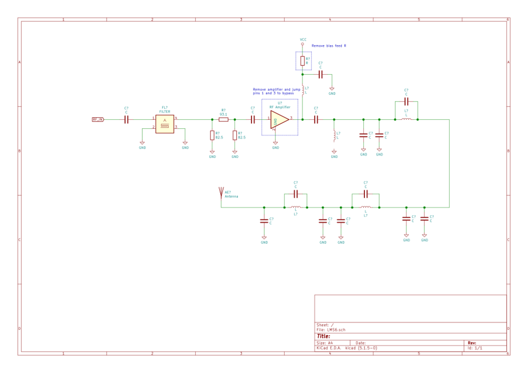
The transmitter RF path contains a filter IC, pi matching network, broadband amplifier, and a few more output filter stages.
Low Pass Filters
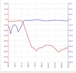
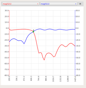
Lowpass Filters are included on the output from the PA and CC1050 to filter out spurs and harmonics from the signal. These are required to meet FCC and NTIA emissions requirements. The measurements were taken with a NanoVNA V2 and the plots were aquired using the NanoVNA-QT software. These data should be considered un-calibrated. A S11 calibration OPEN,SHORT was performed on the NanoVNA, but since the coax is cut, I did not perform an S21 calibration. Additionally, the NanoVNA-QT software seemed to blowaway any of the manual settings I had. This software does not seem to support an OPEN/SHORT only calibration. These data can safely be interpreted as realitive measurements, meaning the filter type and cutoff frequency can be determined.
PA LPF
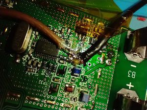
The PA LPF was measured by removing the DC blocking capacitor after the RF amplifier in the schematic above. The removed DC blocking capacitor is Port 1 of the measurement. Port 2 of the measurment is the antenna output with the antenna removed. The 3 dB cutoff of the filter is 500 MHz.
FL101 - CC1050 LPF
The FL101 frequency response was measured as shown below. A DC blocking capacitor was removed that was between the output of CC1050 and FL101. Two parallel resistors were removed from the output of FL101. This isolated the filter in the circuit. The cutoff of the filter is 650 MHz.
Relative Humidity Circuit
Analog Multiplexer
U14 is an 8-channel mux/demux.
- Four of the channels (A0-A3) go to SP1.
- (A4-A7 appear to go to SENS2-4, need to be traced)
- Pin 3 is the common in/out and goes to R13 (560k) and R15 (47k). R15 goes to U15 Pin 7 (555 Reset), and R13 goes to U15 Pin 8 (555 Control.)
- Address Select 0 is connected to ST7 Pin 2 / PB0
- Address Select 1 is connected to ST7 Pin 3 / PB1
- Address Select 2 is connected to ST7 Pin 4 / PB2
Original Firmware
Original firmware is not locked and can be dumped with Rlink-STD Debugger with RFlasher7.
Several dumps are publicly available on https://github.com/MrARM/lms6/tree/master/dumps
Vector table and other interesting addresses:
- 0x9CDB - The start of frequency registers, each dip switch has registers starting from this address.
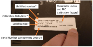
- 0xE003 - Serial number, at least 3 bytes. Ex: 0x7C6A34 is 8153652 big-endian.
- 0xE100 to 0xE136 - something that changes between units. Maybe calibration factors? Checksums?
- 0xFF00 - software string. Ex: "May 17, 2017 - V1.45"
- 0xFFE4 - AVD vector
- 0xFFE6 - SCI / UART vector
- 0xFFE8 - Timer B vector
- 0xFFEA - Timer A vector
- 0xFFEC - SPI vector
- 0xFFEE - vector unused on this chip
- 0xFFF0 - EI3 vector
- 0xFFF2 - EI2 vector
- 0xFFF4 - EI1 vector
- 0xFFF6 - EI0 vector
- 0xFFF8 - MCC/RTC vector
- 0xFFFA - vector unused on this chip
- 0xFFFC - Trap vector
- 0xFFFE - Reset vector
IDA Pro uses CPU type ST7->ST72324J6 during loading, and can load the Intel Hex file produced by the programmer directly for analysis.
Option Bytes
Option bytes are set to 0xE7F7
| Option Description | Original Setting |
|---|---|
| Watchdog Reset on Halt (Reset On Entering Halt) | Reset generation when entering HALT mode |
| Hardware of Software Watchdog | Software (watchdog to be enabled by software) |
| Low Voltage Detection Selection (LVD Config) | Highest Voltage Threshold |
| FLASH read-out protection | Read-out protection disabled |
| Package slection | (A)R - TQFP64 |
| RESET clock cycle selection | Reset phase with 256 CPU cycles |
| Oscillator Type | External Source |
| Oscillator Range | HS 8~16MHz |
| PLL activation | PLL x2 disabled |
GPIO Initialization
- PADDR = 0xF0, PAOR = 0x38 or 0x30 depending on address 0xF3
- PA7: Open Drain Output
- PA6: Open Drain Output
- PA5: Push Pull Output
- PA4: Push Pull Output
- PA3: Depends on address 0xF3
- PBDDR = 0x0F, PBOR=0x1F
- PB4 - Pullup interrupt input
- PB3 - Push Pull Output
- PB2 - Push Pull Output
- PB1 - Push Pull Output
- PB0 - Push Pull Output
- PCDDR = 0x03, PCOR=0x0B
- PC7 - floating input
- PC6 - floating input
- PC5 - floating input
- PC4 - floating input
- PC3 - pullup input
- PC2 - floating input
- PC1 - push pull output
- PC0 - push pull output
- PDDDR = 0x20, PDOR=default to 0x0
- PD5 - open drain output
- PD4 - floating input
- PD3 - floating input
- PD2 - floating input
- PD1 - floating input
- PD0 - floating input
- PFDDR = 0x20 or 0x80 depending on address 0xF3, PFOR=0x10 or 0x80 depending on address 0xF3
- PF7 - depends on 0xF3
- PF6 - floating input - is checked very early on startup and used to set 0xF3. 47k resistor to 5v, TP8, CardEdge21.
- PF5 - depends on 0xF3
- PF4 - depends on 0xF3
- PF2 - floating input
- PF1 - floating input
- PF0 - floating input
MCC Initialization
Done in the main function, MCCSR is initialized to 0x0E. This means:
- Clock Prescaler[CP] is set to /2
- SlowModeSelect[SMS] is set to 0, so CP is ignored and Fcpu=Fosc2
- TimeBase[TB] is 0b11, selecting 25ms timebase
- OscillatorInterruptEnable[OIE] is set, has something to do with low-power mode(s)
- OscillatorInterruptFlag[OIF] is clear, indicates main oscillator has reached countdown
MCCBCR does not appear to be initialized, meaning beeper-mode is disabled.
ADC Configuration
ADCDRL does not appear to be used, thus the ADC is operated as an 8-bit ADC instead of 10-bit.
ST7 ADC AIN8 appears to be the only one used.
Interrupts
- ei0_int
- Triggered by PortA.3
- uses location 0xB2 as a shift register to output LSB first to CC1050's Data Input on PortF.4
- ei3_int
- Triggered by PortB.4
- Sets a variable when GPS PPS occurs
GPS Initialization
On startup, the ST7 sends the following TSIP(0x10 then 0xID, then data with 0x10 double-escaping, then 0x10,0x03) packets to the GPS.
- 0x10, 0x8E, 0x2A, 0x01, 0x10, 0x03 - Request Fix and Channel Tracking Info, Type 1
- 0x10, 0x8E, 0x26, 0x10, 0x03 - SAVE SEEPROM
- 0x10, 0x8E, 0x2B, 0x01, 0x10, 0x03 - Request Fix and Channel Tracking Info, Type 2
- 0x10, 0x8E, 0x26, 0x10, 0x03 - SAVE SEEPROM
Modifications
Disable amplification
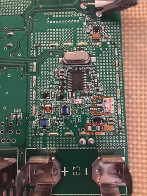
When testing, it's important not to transmit on unlicensed frequencies. Emissions can be eliminated by replacing the RF amplifier with a jumper between pins 1 and 3, and terminating the load at the antenna connection. The amplifier is an SOT-89 device just above the "-" terminal of B3. To access the RF chain, the shield housing may need to be temporarily removed. Also remove the bias feed resistor just below the "L104" marking. Then, remove the transmitter antenna from the "ANT1" connections. Use a 50 ohm resistor across the two terminals to provide a terminating load and eliminate any further transmission. Near-field reception is still possible after making these changes.
Change Frequency[1]
It is possible to change the TX frequency by modifying what is sent to the cc1050(radio) registers. Here is an example on how to get 422.5 MHz
- Download this frequency calculator: https://github.com/rsaxvc/LMS6APRS/blob/master/docs/cc1050%20frequency%20calculator.ods
- The easiest way to get started is to edit NWS1111's frequency(row 17), delete column D and J.
- Change column J to your desired frequency(for this example, 422.500000). Try to keep your frequency close to the original if you want to only have to change the frequency register.
- A number in column I will appear, copy this number to column D and round it up.
- Start gradually adjusting column D until the frequency error (col. K) is around ±5
- Convert your number in column D to hexadecimal
- Acquire a dump of your LMS-6 firmware using a programmer
- Go to 0x9D8F in the dump in a hex editor and insert the first two bytes of your hexadecimal number. Insert the next two after the 05 byte and the final two after the 07 byte.
- Save this hex file and flash it to the LMS-6
- Set all dip switches to 1 1 1 1 and turn on your LMS-6, you should be able to see it transmitting in your desired frequency. If you see abnormalities with the waveform, make sure your Freq Err is good, and check your FSEP and REFDIV values.
Instruction Timing Tables
These are based on the ST Visual Develop 4.3.12 Simulator. Hopefully it is accurate. I've only done the instructions needed for writing a software UART, since the hardware UART is tied up doing GPS work.
| instruction | cycles | Purpose | condition tested |
|---|---|---|---|
| sim | 2 | Set instruction mask(disable interrupts) | |
| nop | 2 | no-op | |
| bres | 5 | bit-reset | ;reset a GPIO pin
BRES PADR, 0 |
| bcp | 2 | bit-compare | BCP A,0 |
| jreq | 3 | jump | jump not taken
jump taken |
| bset | 5 | bit-set | ;set a GPIO pin
BSET PADR, 0 |
| jrt | 3 | jump "right there"? | |
| ld | 2 | load register/memory to/from register/memory | LD A, X |
Ideas for doing AFSK modulation on 70CM with CC1050 and ST7
The goal is to draw an approximation of a sine-wave over time in the frequency domain. This is usually done by drawing a sine-wave with a DAC, low-pass filtering it, and feeding it into an FM modulator, but we don't have those parts.
FeatherHAB Approach using a similar FSK chip
The FeatherHAB approach involves using a transmitter with an asynchronous digital modulation input(CC1050 can do this), and oversamping it like a 1-bit DAC. I think this works as long as the input signal is much faster than the charge pump bandwidth, and if so, it should act like a low-pass filter. FeatherHAB uses a hardware timer to drive their digital modulation input, but they do so by sending a variable-length pulse every 19200 Hz.
We might be able to do this using a 19200Hz periodic timer interrupt to set the modulation pin and a one-shot timer to generate another interrupt to clear it. This will use all available timers on the ST7. We cannot use a timer to generate the pulses directly as the ST7 does not wire out any timers on the right pins.
SFCW-like Frequency Hopping Approach(RSAXVC)
The CC1050 has a pair of frequency register sets, this allows programming a new frequency then flipping to it using a bit - this takes 4x register writes(16 bits each). We could, like a stepped frequency radar, switch between a series of tones rapidly(perhaps 8x symbol rate). This would look like an unfiltered DAC version of a sine-wave with little stair-steps.
Why we're not going to do 9600baud 70CM FSK modulation
For these to be a usable tracker we're going to need ground stations. In the Kansas City metro, there's not many APRS digipeaters on 70cm, and the few there are use 1200 baud AFSK, not 9600 baud FSK.
ST7 Programming
The ST7 can be programmed using the RLINK-STD programmer. This programmer is available from Digi-Key https://www.digikey.com/en/products/detail/iotize/RLINK-STD/9923059
FlashBash Programmer
The FlashBash ST7 programmer claims to be able to program the ST7 on the LMS-6. This has not been evaluated yet. http://www.spen-soft.co.uk/
FlashBash V3 PCB can be ordered from DirtyPCBs.com: https://dirtypcbs.com/store/designer/details/1826/6489/flashbash-v3-st7-programmer
LMS-6 Card Edge Interface
LMS-6 Card edge interface board KiCad schematic and board layout: https://github.com/Reid-n0rc/LMS-6_Interface_Board
LMS-6 Card Edge Interface PCB Rev B can be ordered from DirtyPCBs.com: https://dirtypcbs.com/store/designer/details/1826/6490/lms6-interface-board-rev-b
| Manufacturer Part Number | Manufacturer | Digi-Key Part Number | Customer Reference | Reference Designator | Packaging | Part Status | Quantity | Unit Price | Extended Price | Quantity Available | Mfg Std Lead Time | Description | RoHS Status | Lead Free Status | REACH Status |
|---|---|---|---|---|---|---|---|---|---|---|---|---|---|---|---|
| 885012207095 | Würth Elektronik | 732-8077-1-ND | C4 | C4 | Cut Tape (CT) | Active | 2 | 0.1 | $0.20 | 4457 | 12 Weeks | CAP CER 0.033UF 50V X7R 0805 | ROHS3 Compliant | Lead free | REACH Unaffected |
| CL21B104KBCNNNC | Samsung Electro-Mechanics | 1276-1003-1-ND | C3,C5,C6 | C3,C5,C6 | Cut Tape (CT) | Active | 4 | 0.1 | $0.40 | 2366592 | 22 Weeks | CAP CER 0.1UF 50V X7R 0805 | ROHS3 Compliant | Lead free | REACH Unaffected |
| T491A106K010AT | KEMET | 399-3684-1-ND | C7 | C7 | Cut Tape (CT) | Active | 1 | 0.33 | $0.33 | 4400267 | 7 Weeks | CAP TANT 10UF 10% 10V 1206 | ROHS3 Compliant | Lead free | REACH Unaffected |
| CL31A106KAHNNNE | Samsung Electro-Mechanics | 1276-1075-1-ND | C8 | C8 | Cut Tape (CT) | Active | 2 | 0.2 | $0.40 | 1387438 | 22 Weeks | CAP CER 10UF 25V X5R 1206 | ROHS3 Compliant | Lead free | REACH Unaffected |
| CL31B475KAHNNNE | Samsung Electro-Mechanics | 1276-1055-1-ND | C9 | C9 | Cut Tape (CT) | Active | 1 | 0.2 | $0.20 | 124045 | 22 Weeks | CAP CER 4.7UF 25V X7R 1206 | ROHS3 Compliant | Lead free | REACH Unaffected |
| LH R974-LP-1 | OSRAM Opto Semiconductors Inc. | 475-1415-1-ND | D1 | D1 | Cut Tape (CT) | Active | 2 | 0.25 | $0.50 | 89674 | 12 Weeks | LED RED DIFFUSED 0805 SMD | ROHS3 Compliant | Lead free | REACH Unaffected |
| LG R971-KN-1 | OSRAM Opto Semiconductors Inc. | 475-1410-1-ND | D2, D3 | D2, D3 | Cut Tape (CT) | Active | 2 | 0.25 | $0.50 | 325681 | 12 Weeks | LED GREEN DIFFUSED 0805 SMD | ROHS3 Compliant | Lead free | REACH Unaffected |
| MPZ2012S601AT000 | TDK Corporation | 445-2206-1-ND | FB1, FB2 | FB1, FB2 | Cut Tape (CT) | Active | 2 | 0.11 | $0.22 | 228257 | 10 Weeks | FERRITE BEAD 600 OHM 0805 1LN | ROHS3 Compliant | Lead free | REACH Unaffected |
| 105-1103-001 | Cinch Connectivity Solutions Johnson | J577-ND | J1-J12 | J1,J12 | Bulk | Active | 2 | 0.73 | $1.46 | 15970 | 7 Weeks | CONN TIP JACK SOLDER BLACK | RoHS Compliant | Lead free | Not Available |
| 61300311121 | Würth Elektronik | 732-5316-ND | J2,J6,J10 | J2,J6,J10 | Bag | Active | 3 | 0.13 | $0.39 | 73107 | 13 Weeks | CONN HEADER VERT 3POS 2.54MM | ROHS3 Compliant | Lead free | REACH Unaffected |
| 105-1102-001 | Cinch Connectivity Solutions Johnson | J576-ND | J3,J11 | Bulk | Active | 2 | 1.05 | $2.10 | 0 | 7 Weeks | CONN TIP JACK SOLDER RED | RoHS Compliant | Lead free | Not Available | |
| UJ2-MIBH-4-SMT-TR | CUI Devices | 102-4006-1-ND | J4 | J4 | Cut Tape (CT) | Active | 1 | 0.79 | $0.79 | 47066 | 11 Weeks | CONN RCPT USB2.0 MICRO B SMD R/A | RoHS Compliant | Lead free | Not Available |
| 302-S101 | On Shore Technology Inc. | ED1543-ND | J7 | J7 | Bulk | Active | 1 | 0.28 | $0.28 | 29961 | 9 Weeks | CONN HEADER VERT 10POS 2.54MM | ROHS3 Compliant | Lead free | REACH Unaffected |
| PREC018DAAN-RC | Sullins Connector Solutions | S2012EC-18-ND | J9 | J9 | Bag | Active | 1 | 0.69 | $0.69 | 1395 | Not Available | CONN HEADER VERT 36POS 2.54MM | ROHS3 Compliant | Lead free | REACH Unaffected |
| 61300211121 | Würth Elektronik | 732-5315-ND | J13 | J13 | Bag | Active | 1 | 0.13 | $0.13 | 127153 | 13 Weeks | CONN HEADER VERT 2POS 2.54MM | ROHS3 Compliant | Lead free | REACH Unaffected |
| NPC02SXON-RC | Sullins Connector Solutions | S9341-ND | JUMPER | Bag | Active | 4 | 0.11 | $0.44 | 209938 | 5 Weeks | CONN JUMPER SHORTING .100" GOLD | ROHS3 Compliant | Lead free | REACH Unaffected | |
| RC1206JR-070RL | Yageo | 311-0.0ERCT-ND | L1 - Replacement | L1 | Cut Tape (CT) | Active | 1 | 0.1 | $0.10 | 9627917 | 24 Weeks | RES SMD 0 OHM JUMPER 1/4W 1206 | ROHS3 Compliant | Lead free | REACH Unaffected |
| EBC20DRAS | Sullins Connector Solutions | S9672-ND | J5 | J5 | Tray | Active | 1 | 6.9 | $6.90 | 0 | 3 Weeks | CONN EDGE DUAL FMALE 40POS 0.100 | ROHS3 Compliant | Lead free | REACH Unaffected |
| CRG0805F27R | TE Connectivity Passive Product | A126357CT-ND | R1,R2 | Cut Tape (CT) | Active | 2 | 0.1 | $0.20 | 30073 | 18 Weeks | RES SMD 27 OHM 1% 1/8W 0805 | RoHS Compliant | Lead free | Not Available | |
| CRGCQ0805F1K5 | TE Connectivity Passive Product | A129751CT-ND | R3 | Cut Tape (CT) | Active | 2 | 0.1 | $0.20 | 46326 | 21 Weeks | CRGCQ 0805 1K5 1% | RoHS Compliant | Lead free | Not Available | |
| RC1005F103CS | Samsung Electro-Mechanics | 1276-3431-1-ND | R4 | Cut Tape (CT) | Discontinued at Digi-Key | 2 | 0.1 | $0.20 | 8019 | Not Available | RES SMD 10K OHM 1% 1/16W 0402 | ROHS3 Compliant | Lead free | REACH Unaffected | |
| RC0805JR-07470RL | Yageo | 311-470ARCT-ND | R5 | Cut Tape (CT) | Active | 2 | 0.1 | $0.20 | 823055 | 24 Weeks | RES SMD 470 OHM 5% 1/8W 0805 | ROHS3 Compliant | Lead free | REACH Unaffected | |
| RC0805FR-07470KL | Yageo | 311-470KCRCT-ND | R6 | Cut Tape (CT) | Active | 2 | 0.1 | $0.20 | 665330 | 24 Weeks | RES SMD 470K OHM 1% 1/8W 0805 | ROHS3 Compliant | Lead free | REACH Unaffected | |
| ERJ-6ENF1373V | Panasonic Electronic Components | P137KCCT-ND | R7 | Cut Tape (CT) | Active | 2 | 0.1 | $0.20 | 95215 | 11 Weeks | RES SMD 137K OHM 1% 1/8W 0805 | ROHS3 Compliant | Lead free | REACH Unaffected | |
| RC0805FR-0754K9L | Yageo | 311-54.9KCRCT-ND | R8 | Cut Tape (CT) | Active | 2 | 0.1 | $0.20 | 19069 | 24 Weeks | RES SMD 54.9K OHM 1% 1/8W 0805 | ROHS3 Compliant | Lead free | REACH Unaffected | |
| ERJ-6ENF1621V | Panasonic Electronic Components | P1.62KCCT-ND | R9 | Cut Tape (CT) | Active | 1 | 0.1 | $0.10 | 220523 | 11 Weeks | RES SMD 1.62K OHM 1% 1/8W 0805 | ROHS3 Compliant | Lead free | REACH Unaffected | |
| ERJ-6ENF1433V | Panasonic Electronic Components | P143KCCT-ND | R10 | Cut Tape (CT) | Active | 1 | 0.1 | $0.10 | 34393 | 11 Weeks | RES SMD 143K OHM 1% 1/8W 0805 | ROHS3 Compliant | Lead free | REACH Unaffected | |
| RC0805FR-07280RL | Yageo | 311-280CRCT-ND | R11 | Cut Tape (CT) | Active | 2 | 0.1 | $0.20 | 180886 | 24 Weeks | RES SMD 280 OHM 1% 1/8W 0805 | ROHS3 Compliant | Lead free | REACH Unaffected | |
| RC0805FR-07909RL | Yageo | 311-909CRCT-ND | R12 | Cut Tape (CT) | Active | 2 | 0.1 | $0.20 | 284632 | 24 Weeks | RES SMD 909 OHM 1% 1/8W 0805 | ROHS3 Compliant | Lead free | REACH Unaffected | |
| RC0805FR-071ML | Yageo | 311-1.00MCRCT-ND | R13 | Cut Tape (CT) | Active | 2 | 0.1 | $0.20 | 2662481 | 24 Weeks | RES SMD 1M OHM 1% 1/8W 0805 | ROHS3 Compliant | Lead free | REACH Unaffected | |
| FT2232D-REEL | FTDI, Future Technology Devices International Ltd | 768-1010-1-ND | U1 | Cut Tape (CT) | Active | 1 | 6.99 | $6.99 | 24630 | 11 Weeks | IC USB FS DUAL UART/FIFO 48-LQFP | RoHS Compliant | Lead free | REACH Unaffected | |
| TEC 2-1219WI | Traco Power | 1951-1401-ND | U2 | Tube | Active | 1 | 10.26 | $10.26 | 13 | 13 Weeks | DC DC CONVERTER 9V 2W | ROHS3 Compliant | Lead free | Not Available | |
| CSTNR6M00GH5C000R0 | Murata Electronics | 490-18276-1-ND | Y1 | Cut Tape (CT) | Active | 1 | 0.44 | $0.44 | 7201 | 11 Weeks | CERAMIC RES 6.0000MHZ 39PF SMD | ROHS3 Compliant | Not Available | Not Available | |
| TPS25921ADR | Texas Instruments | 296-40731-1-ND | U3 | Cut Tape (CT) | Active | 1 | 1.45 | $1.45 | 36658 | 6 Weeks | IC PWR MGR EFUSE 18V 8SOIC | ROHS3 Compliant | Lead free | REACH Unaffected |
Interface Description and Theory of Operation
The LMS-6 interface PCB allows the LMS-6 to be powered, connect to USB to UART, and connect to an in circuit programmer through the card edge connector.
| Jumper Ref Des | Jumpered Pins | |||
|---|---|---|---|---|
| Battery | USB 5V | Banana Jacks Regulated (J1&J3) | Direct Power (J11&J12) | |
| J2 | X | 2,3 | 1,2 | X |
| J6 | 1,2 | 2,3 | 2,3 | 2,3 |
| J10 | X | 2,3 | 2,3 | 1,2 |
LMS-6 Interface Board Schematic Rev 10
Circuit Power Options
The LMS-6 Inteface board offers four power options to power LMS-6. Components for any of the power options can be omitted if they will be unused to reduce the build the build cost.
Battery Power
The LMS-6 can be powered using three CR123 lithium batteries connected to the LMS-6 onboard battery holders. Batter power is enabled by jumpering Pin 1 and Pin to of J6 together.
USB 5V Power
The LMS-6 can be powered from the J4 Micro USB B connection. This is enabled by jumpering Pin 2 and Pin 3 of J2; Pin 2 and Pin 3 of J6.
USB power is indicated by D2 Green LED
USB to UART
The LMS-6 interface includes a FT-2232 USB to UART. UART1 is connected to GPS. The default baud rate for the GPS is 38400 bps. UART 2 TX is connected to U3 pin 19 on the LMS-6.
If the connections are wrong, they can swapped using JP1,JP2 and JP4, JP5.
In Circuit Programming
eFuse
Reference
Here are some reference materials. This is an initial population of material, and this section will need significant cleanup - putting links up for now.
https://www.weather.gov/media/upperair/Documents/RWS_Build_3.4_User_Manual_%20071818.pdf - Radiosonde Replacement System Workstation User Guide. This manual describes the operational environment of the radiosonde.
https://www.nws.noaa.gov/directives/010/pd01014001b.pdf - Rawinsonde Operations - some more technical data on radiosonde operations.
