Difference between revisions of "LMS-6 Radiosonde"
Paul Rixon (talk | contribs) (→Relative Humidity Circuit: (m) Converted schematic sketch to SVG drawing) |
(Add notes about 16MHz crystal and clock buffer) |
||
| Line 293: | Line 293: | ||
''U11 - (Marked 73RW, SOT-89 or similar) - Pre-amp for GPS ant? In GPS section can.'' | ''U11 - (Marked 73RW, SOT-89 or similar) - Pre-amp for GPS ant? In GPS section can.'' | ||
| − | ''U12 - (Marked G5/849)'' | + | ''U12 - (Marked G5/849) - looks like a clock buffer between Y3 and U3'' |
'''U13''' - [http://web.archive.org/web/20200214104034/http://www.ti.com/lit/ds/symlink/cd4040b.pdf CD4040BPW] - 12-stage Ripple-Carry Binary Counter/Divider <ref group="IC Footnotes" name="U13">Package marking shows CM040B. TI Park marking lookup provides CD4040BPW.</ref> | '''U13''' - [http://web.archive.org/web/20200214104034/http://www.ti.com/lit/ds/symlink/cd4040b.pdf CD4040BPW] - 12-stage Ripple-Carry Binary Counter/Divider <ref group="IC Footnotes" name="U13">Package marking shows CM040B. TI Park marking lookup provides CD4040BPW.</ref> | ||
| Line 317: | Line 317: | ||
''Unot_marked (23/24?) - (Marked W6K/W76) - RF Amp, similar to SKY65013-70LF (No designator; under TX can to bottom-right of U21.)'' | ''Unot_marked (23/24?) - (Marked W6K/W76) - RF Amp, similar to SKY65013-70LF (No designator; under TX can to bottom-right of U21.)'' | ||
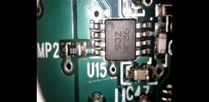
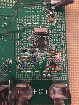
| − | '''U25''' - [http://web.archive.org/web/20200123234645/https://www.ti.com/lit/ds/symlink/tps72.pdf TPS7201Q] - Adj. 1.2-9.75V LDO - (Designator silkscreen is hard to read; 8-SOIC on bottom-right)[[File:U?? - TPS7201Q.jpg|none|thumb|U25 and general area]] | + | '''U25''' - [http://web.archive.org/web/20200123234645/https://www.ti.com/lit/ds/symlink/tps72.pdf TPS7201Q] - Adj. 1.2-9.75V LDO - (Designator silkscreen is hard to read; 8-SOIC on bottom-right) |
| + | |||
| + | '''Y3''' - 16MHz crystal[[File:U?? - TPS7201Q.jpg|none|thumb|U25 and general area]] | ||
[[File:Screenshot 20200904-195417.png|thumb|92JK ZC5 chip noted as U15|alt=|none]] | [[File:Screenshot 20200904-195417.png|thumb|92JK ZC5 chip noted as U15|alt=|none]] | ||
{| class="wikitable" | {| class="wikitable" | ||
Revision as of 02:14, 27 September 2020
The LMS-6 Radiosonde is a radiosonde manufactured by Lockheed-Martin Sippican, and used for meteorological sounding.
Contents
Overview
There are two models of the LMS-6, a 403MHz model and a 1680MHz model. This article will cover the 403MHz model unless specified.
Specs
- 16 Fixed transmit carrier frequencies (MHz): 400.250, 400.625, 401.000, 401.375, 401.750, 402.125, 402.500, 402.875, 403.250, 403.625, 404.000, 404.375, 404.750, 405.125, 405.500, 405.875
- Frequency tolerance +/-30ppm
- Mean TX Power 70.8mW (18.5dBm)
- Emission Designator 16K8F1D
- FSK with a maximum modulating frequency of 4.8 kHz
- Emission 3dB BW +/-5.0 kHz
- Emission 20dB BW +/-12.7 kHz
- Omnidirectional antenna
- Main beam gain 2dBi
- Horizontal Beamwidth 360 degrees
- Vertical Beamwidth +84 degrees
Source: https://apps.fcc.gov/els/GetAtt.html?id=121623&x=.
Photos
Connectors
There are four sensor connectors (SENSN) used for sensor input by the radiosonde. SENS1 is not populated on the 403MHz units. SENS2-4 have leads connected to them, and the sensors are connected to the other end of the leads, outside of the radiosonde housing. Only SENS1 appears to have spacing for a connector; the others have arbitrary lead spacing.
| Pin | Characteristics |
|---|---|
| 1 | +5V (5.47 measured) - From U25 |
| 2 | GND |
| 3 | U3 Pin 37 (PA7, High Sink/20mA) |
| 4 | 1 Hz - U14 Pin 9 (S2) |
| 5 | 1 Hz - U14 Pin 11 (S1) |
| 6 | 1 Hz - U14 Pin 11 (S0) |
| 7 | Pulldown via R41 (47k) to GND |
Public information shows this header may be used for adding additional analog sensors to the radiosonde.
| Pin | Connection |
|---|---|
| 1 | Sensor pin 1 |
| 2 | Sensor pin 2 |
0.3" spacing. Both lead wires have ferrite beads immediately before connecting to the board.
| Pin | Connection |
|---|---|
| 1 | Sensor pin 1 |
| 2 | Sensor pin 2 |
0.5" spacing.
| Pin | Connection |
|---|---|
| 1 | Sensor pin 1 |
| 2 | Sensor pin 2 |
0.3" spacing. Fine gauge insulated wire run along SENS3 wire and loomed in white heat-shrink tubing.
| Pin Number | Function | Notes / Observations |
|---|---|---|
| 1,2,7,8 | U3 - Vdd | U15 - Pin 4 | |
| 9, 10, 15, 16, 19, 20, 33, 34 | Ground | |
| 2, 8, 18*, 24, 30 | +5VDC | 18 needs more research, may occasionally drop to ground? |
| 3 | U3 - ICCLK | TP33 | U21 - PCLK | |
| 4 | U3 - Vpp/ICCSEL | |
| 5 | U3 - RESET | |
| 6 | U3 - ICCDATA | |
| 11 | J5 - Pin 2 | |
| 12 | 3.3v - 2.5KHz square wave (4msec p/p) | |
| 13 | U3 - SW1.4 | |
| 17 | U3 - SW1.2 | |
| 18 | U3 - SW1.1 | |
| 23 | Rounded-square wave data bursts | |
| 26 | Rounded-square wave data bursts | |
| 31 | BATT POS | |
| 36 | U3 - SW1.3 | |
| 38 | U3 - OCMP1_A / AIN10 / PF4 | Square wave data bursts, 0.2msec per bit |
| 39 | RED WIRE | |
| 40 | Battery voltage | Around 9VDC measured |
| Pin | Wire Color | Use |
|---|---|---|
| 1 | Black | Ground |
| 2 | White | Battery +9 |
| 3 | Red | +9 VDC In |
| 4 | NC | Unknown - goes to
unpopulated CR1 |
J4 - NC - earphone jack? uses SENS3 leads
| Pin | Use |
|---|---|
| 1 | Unknown |
| 2 | Unknown |
| 3 | Unknown |
| 4 | Unknown |
These traces go to U3 (ST microcontroller)
| Pin | Use | Notes/Observations |
|---|---|---|
| 1 | +5VDC | |
| 2 | Unknown | U14 Pin 13 (A0) - 3V rounded square pulses, 2x per second, 2 different periods avg ~75msec? |
| 3 | +5VDC | |
| 4 | Unknown | U14 Pin 14 (A1) - 5V, 0.1msec pulse once per second |
| 5 | +5VDC | |
| 6 | Unknown | U14 Pin 15 (A2) - 5V, 0.1msec pulse once per second |
| 7 | +5VDC | |
| 8 | Unknown | U14 Pin 12 (A3) - 3V, 250msec pulse once per second |
SP1 connects to four channels of U14, an 8-channel analog MUX. Pin 2 also connects to R111, non-populated, which would provide a pull-up to +5 at Pin 1.
Components
The following is a catalog of active components. Designators italicized still need positive identification; bold have been positively identified. Markings listed where known to help in identification. List additional markings when they differ.
U1 - GPS - Trimble 63530-50 - 12-channel GPS, 2x serial ports, 2.7-3.3VDC, SBAS, flash almanac/ephemeris/location storage. (The -50 variant is probably a custom variant, and exact capabilities are unknown.)
U2 - (Marked G4/905)
U3 - ST72F324J6T6 - 32K Flash, 1K RAM, 5VDC, 10-bit ADC (16 inputs, muxed), 4x Timer, SPI, SCI, 32-bits total I/O
- 72F324J6T6 - ST72324 - Main Microcontroller, ST7 series Datasheet
- ST7 Flash Programming Quick Reference Guide
- ST7 Family Flash Programming Reference Manual
- ST7 Family ICC Protocol Reference Manual
U4 - (Marked Z252)
U5, U6 - LP2985 - LDO - 2.8V?
U7 - (Marked G4/905)
U8 - (Marked G4/905)
U9 - (Marked F50)
U10 - (Did not locate, maybe not placed?)
U11 - (Marked 73RW, SOT-89 or similar) - Pre-amp for GPS ant? In GPS section can.
U12 - (Marked G5/849) - looks like a clock buffer between Y3 and U3
U13 - CD4040BPW - 12-stage Ripple-Carry Binary Counter/Divider [IC Footnotes 1]
U14 - CD74HC4051PWR - High-Speed CMOS Logic Analog Mux/Demux - 8:1
U15 - TI LMC555CMM Family [IC Footnotes 2]
U16 - LMV761MF - Low Voltage Precision Comparator w/ Push-Pull Output [IC Footnotes 3]
U17 - (Marked Z252)
U18 - (Did not locate, maybe not placed?)
U19 - (Did not locate, maybe not placed?)
U20 - Toshiba TC7WH157FU
U21 - CC1050 (back) - Low Power Transmitter - 300MHz-1000MHz, variable power, FSK
U22 - TPS79133DBUR - 3.3V LDO - for U21
Unot_marked (23/24?) - (Marked W6K/W76) - RF Amp, similar to SKY65013-70LF (No designator; under TX can to bottom-right of U21.)
U25 - TPS7201Q - Adj. 1.2-9.75V LDO - (Designator silkscreen is hard to read; 8-SOIC on bottom-right)
Y3 - 16MHz crystal
| U15 Pin | Function | Observations/Notes |
|---|---|---|
| 1 | GND | |
| 2 | 5VDC | |
| 3 | Trigger | Rounded square wave (maybe sawtooth) alternating between 2msec and 4msec, resting at +3VDC between bursts |
| 4 | Discharge | Rounded square wave alternating between 3msec and 5msec, short periods of 0v, resting at +3VDC between bursts |
| 5 | Output | Data. Square wave. 5V space, 0v mark? Pulses around 250msec per bit. |
| 6 | Threshold | More rounded square wave bursts |
| 7 | Reset | |
| 8 | Control |
Sens 4 - Capacitive Relative humidity sensor [IC Footnotes 4]
Notes
- ↑ Package marking shows CM040B. TI Park marking lookup provides CD4040BPW.
- ↑ IC marked with ZC5. TI Part marking lookup provides LMV761. Pinout, footprint, and measured IC/pin operation matches what is expected from a 555.
- ↑ Package marking shows C22A. TI Part marking lookup provides LMV761. The SOT-23 footprint appears to match what is on the PCB.
- ↑ Sens 4 is known to be capacitive since it is listed as such on page 13 of the WMO Common Code Tables Document
Test Points
TP58 - MUX in/out (U14 Pin 3)
Circuits
RF Transmitter Circuit
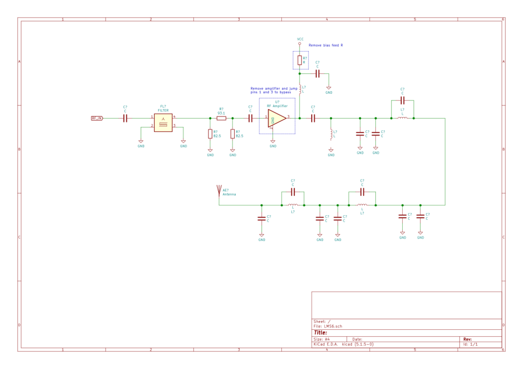
The transmitter RF path contains a filter IC, pi matching network, broadband amplifier, and a few more output filter stages.
Low Pass Filters
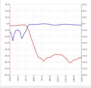
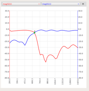
Lowpass Filters are included on the output from the PA and CC1050 to filter out spurs and harmonics from the signal. These are required to meet FCC and NTIA emissions requirements. The measurements were taken with a NanoVNA V2 and the plots were aquired using the NanoVNA-QT software. These data should be considered un-calibrated. A S11 calibration OPEN,SHORT was performed on the NanoVNA, but since the coax is cut, I did not perform an S21 calibration. Additionally, the NanoVNA-QT software seemed to blowaway any of the manual settings I had. This software does not seem to support an OPEN/SHORT only calibration. These data can safely be interpreted as realitive measurements, meaning the filter type and cutoff frequency can be determined.
PA LPF
The PA LPF was measured by removing the DC blocking capacitor after the RF amplifier in the schematic above. The removed DC blocking capacitor is Port 1 of the measurement. Port 2 of the measurment is the antenna output with the antenna removed. The 3 dB cutoff of the filter is 500 MHz.
FL101 - CC1050 LPF
The FL101 frequency response was measured as shown below. A DC blocking capacitor was removed that was between the output of CC1050 and FL101. Two parallel resistors were removed from the output of FL101. This isolated the filter in the circuit. The cutoff of the filter is 650 MHz.
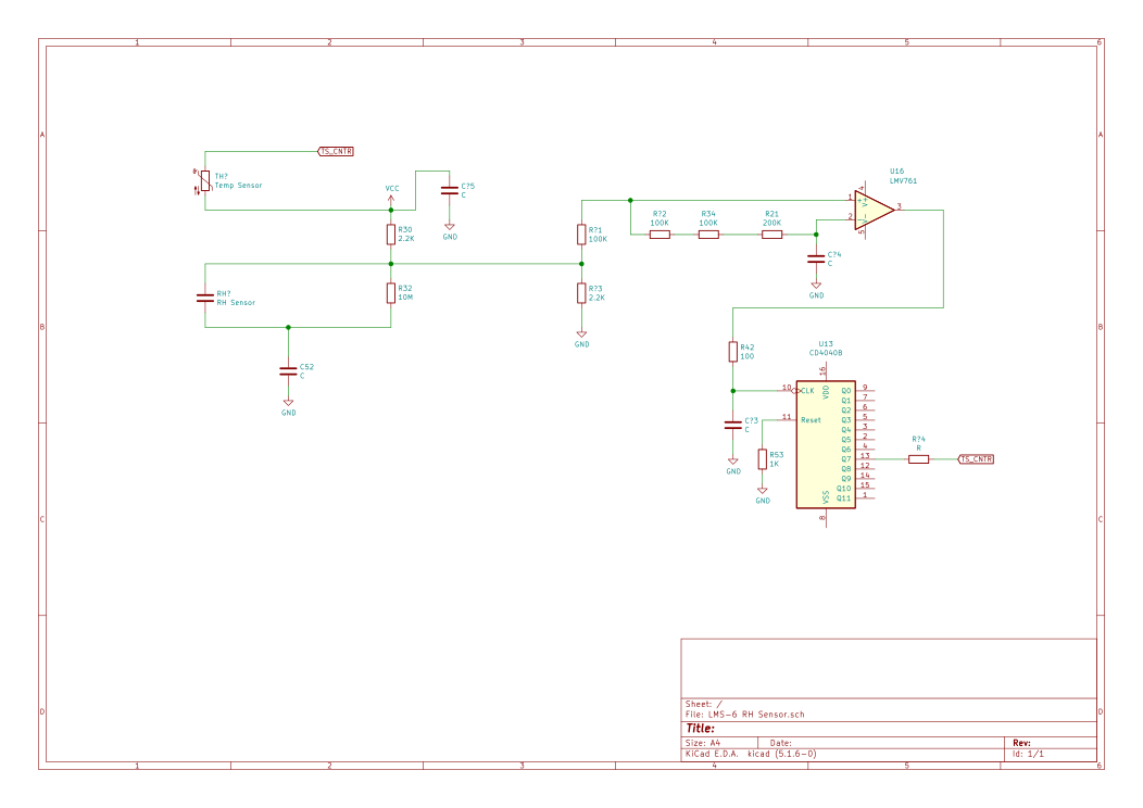
Relative Humidity Circuit
Analog Multiplexer
U14 is an 8-channel mux/demux. Four of the channels (A0-A3) go to SP1. (A4-A7 appear to go to SENS2-4, need to be traced) Pin 3 is the common in/out, and goes to R13 (560k) and R15 (47k). R15 goes to U15 Pin 7 (555 Reset), and R13 goes to U15 Pin 8 (555 Control.)
Modifications
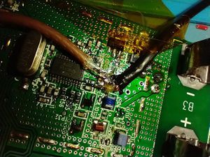
Disable amplification
When testing, it's important not to transmit on unlicensed frequencies. Emissions can be eliminated by replacing the RF amplifier with a jumper between pins 1 and 3, and terminating the load at the antenna connection. The amplifier is an SOT-89 device just above the "-" terminal of B3. To access the RF chain, the shield housing may need to be temporarily removed. Also remove the bias feed resistor just below the "L104" marking. Then, remove the transmitter antenna from the "ANT1" connections. Use a 50 ohm resistor across the two terminals to provide a terminating load and eliminate any further transmission. Near-field reception is still possible after making these changes.
