Difference between revisions of "Kenwood TH-D74A"
| (38 intermediate revisions by the same user not shown) | |||
| Line 1: | Line 1: | ||
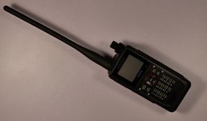
| − | [[File:TH-D74A.jpg | + | [[File:TH-D74A.jpg|thumb|Fully Assembled Kenwood TH-D74A|alt=]]Full teardown pictures and videos of the TH-D74 along with notes on reverse engineering and obtaining a copy of the firmware. |
| + | |||
==Teardown Video== | ==Teardown Video== | ||
| − | + | 6 minute video @ 3x playback speed showing full disassembly of the radio with commentary, full length video with no audio [https://youtu.be/Q_n_bs6f8gE here]. | |
| − | <youtube width="320" height="240"> | + | <youtube width="320" height="240">Q_n_bs6f8gE</youtube> |
==Teardown PCB Pictures== | ==Teardown PCB Pictures== | ||
| − | <gallery mode="packed | + | <gallery mode="packed" widths="300" heights="200"> |
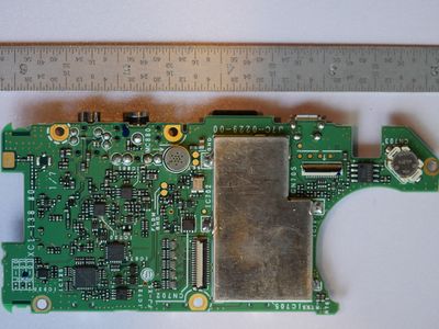
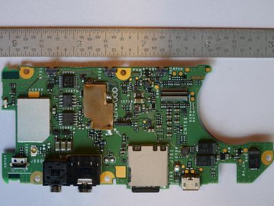
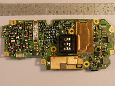
File:TH-D74A Processor board Top.jpg|Processor Board Top | File:TH-D74A Processor board Top.jpg|Processor Board Top | ||
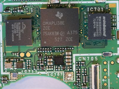
File:TH-D74A Processor.jpg|Processor Shield Removed | File:TH-D74A Processor.jpg|Processor Shield Removed | ||
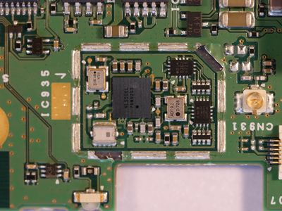
| + | File:TH-D74A GPS Circuit.JPG|GPS circuit normally under a shield. | ||
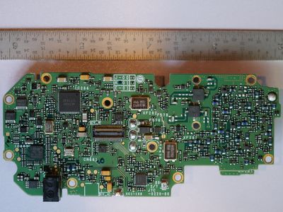
File:TH-D74A Processor board bottom.jpg|Processor Board Bottom | File:TH-D74A Processor board bottom.jpg|Processor Board Bottom | ||
| − | |||
File:TH-D74A Transceiver board top.jpg|Transceiver Board Top | File:TH-D74A Transceiver board top.jpg|Transceiver Board Top | ||
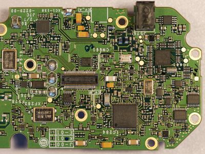
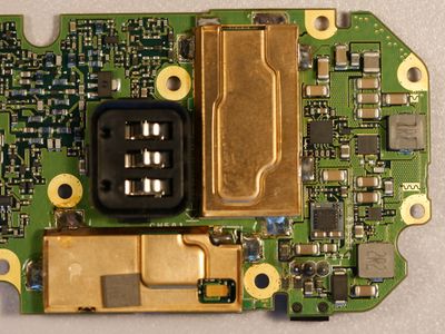
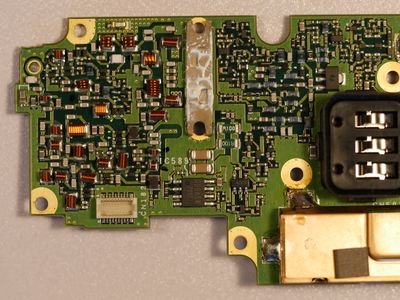
File:TH-D74A Transceiver board top zoom 1.jpg|Transceiver Board Top Zoom 1 | File:TH-D74A Transceiver board top zoom 1.jpg|Transceiver Board Top Zoom 1 | ||
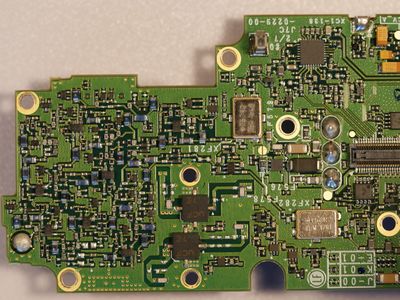
| Line 19: | Line 20: | ||
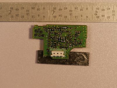
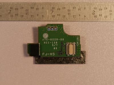
File:TH-D74A FJ-X5 bottom.jpg|FM Radio Module Bottom | File:TH-D74A FJ-X5 bottom.jpg|FM Radio Module Bottom | ||
</gallery> | </gallery> | ||
| + | ==Port and Test Point Identification== | ||
| + | <gallery mode="packed" heights="200"> | ||
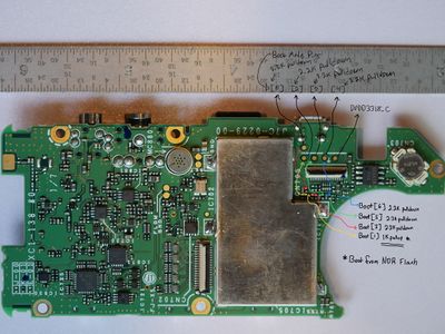
| + | File:Kenwood TH-D74 Control Board Boot Pins.jpeg|Test point locations for Boot[] pins which set the boot-up mode of the OMAP L138 processor, in this case to boot from NOR Flash. | ||
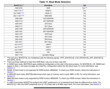
| + | File:OMAP L138 Boot Mode Selection.jpeg|OMAP L138 Boot Mode Selection, TH-D74 is set to boot into NOR Flash at the top of the list. | ||
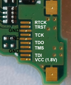
| + | File:TH-D74A JTAG Pinout.png|JTAG pinout | ||
| + | </gallery><br /> | ||
==Modules and Interconnects== | ==Modules and Interconnects== | ||
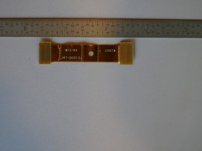
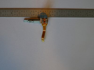
| − | <gallery mode="packed | + | <gallery mode="packed" heights="200"> |
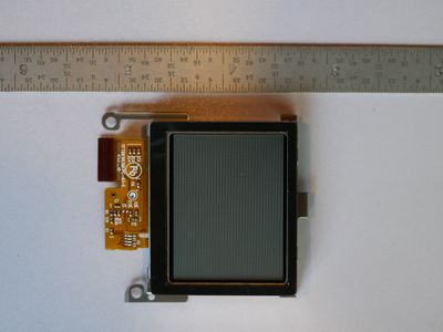
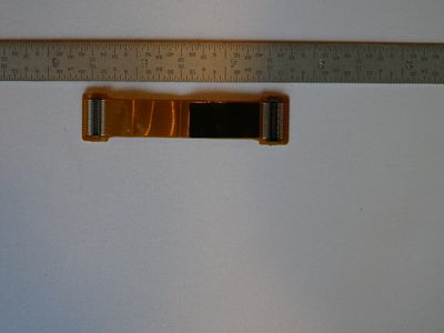
File:TH-D74A LCD front.jpg|LCD Front | File:TH-D74A LCD front.jpg|LCD Front | ||
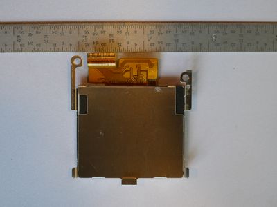
File:TH-D74A LCD back.jpg|LCD Back | File:TH-D74A LCD back.jpg|LCD Back | ||
| Line 31: | Line 38: | ||
==Mechanical Pictures== | ==Mechanical Pictures== | ||
| − | <gallery mode="packed | + | <gallery mode="packed" heights="200"> |
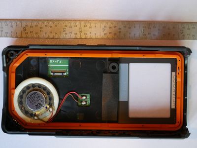
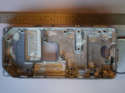
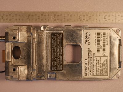
File:TH-D74A Front case interior.jpg|Front Case Interior | File:TH-D74A Front case interior.jpg|Front Case Interior | ||
File:TH-D74A Metal Frame front.jpg|Metal Frame Front | File:TH-D74A Metal Frame front.jpg|Metal Frame Front | ||
| Line 40: | Line 47: | ||
File:TH-D74A Rubber.jpg|Rubber Gaskets | File:TH-D74A Rubber.jpg|Rubber Gaskets | ||
File:TH-D74A Screws.jpg|Screws and Knobs | File:TH-D74A Screws.jpg|Screws and Knobs | ||
| − | </gallery>< | + | </gallery> |
| + | ==Reverse Engineering Efforts== | ||
| + | [[File:Kenwood TH-D74 and JTAGulator.jpg|none|thumb|Kenwood TH-D74 connected to JTAGulator]] | ||
| + | |||
| + | ===High level goals=== | ||
| + | |||
| + | *Obtain a copy of the firmware for analysis/modification | ||
| + | *Understand how the radio works and what test ports are available internally | ||
| + | |||
| + | ====Obtaining firmware==== | ||
| + | |||
| + | *Determine routes of attack | ||
| + | **JTAG Port | ||
| + | **Serial Port | ||
| + | **Hardware attack - Remove Flash Memory and read directly (possibly encrypted/obfuscated) | ||
| + | **USB data capture - Packet capture firmware update (possibly encrypted/obfuscated) | ||
| + | |||
| + | Initially the radio was opened and wires were soldered to some test points and an interesting PCB footprint that I suspected was JTAG as seen in the video below. | ||
| + | |||
| + | <youtube width="320" height="240">EZP2DVU9IvQ</youtube> | ||
| + | |||
| + | =====Serial Port===== | ||
| + | The serial port turned out to just be control data sent from the CPU board to the transceiver board, explained further below. Removing the flash memory is an option although it is a BGA package so not sure about soldering wires to it so it can be read out. Furthermore, the OMAP-L138 processor seems to have a few protection mechanisms. Encryption of the firmware is one of them so that route might be useless. | ||
| + | |||
| + | ====Hardware Attack==== | ||
| + | |||
| + | *Desolder flash memory chip | ||
| + | *Re-Ball BGA and clean in preparation for socket | ||
| + | *Insert into BGA socket and read contents using [https://www.embeddedcomputers.net/products/FlashcatUSB_XPORT/ FlashCATUSB XPORT] with [https://www.embeddedcomputers.net/products/ParallelAdapters/ BGA-64 (LAE064)] socket | ||
| + | |||
| + | Other than the obvious challenge of desoldering and reballing a BGA, this worked great to get a complete image of the firmware! The firmware on the flash is not encrypted or obfuscated in any way so it's possible to make use of it immediately. | ||
| + | |||
| + | Cost breakdown to get complete firmware image using this method: '''$330 USD''' | ||
| + | |||
| + | *$145 - Replacement Processor board for TH-D74 (eBay) | ||
| + | *$40 - [https://www.embeddedcomputers.net/products/FlashcatUSB_XPORT/ FlashcatUSB XPORT] | ||
| + | *$145 - [https://www.embeddedcomputers.net/products/ParallelAdapters/ BGA-64 (LAE064)] Socket | ||
| + | |||
| + | Having a copy of the firmware for modification and analysis... PRICELESS! | ||
| + | |||
| + | ====USB Data Capture==== | ||
| + | This method costs a lot less than the hardware attack, like $330 less! See the YouTube video below for a walk-through. The software tools used are listed below, I am sure other tools would work but this is what I used. | ||
| + | |||
| + | '''''Have a better method? Create an account and update the wiki!''''' | ||
| + | |||
| + | <youtube width="320" height="240">BwFnZOvw0wk</youtube> | ||
| + | |||
| + | [https://www.hhdsoftware.com/hex-editor Hex Editor Neo] - Allows bitwise operations and other cool features with a 14 day free trial! | ||
| + | |||
| + | [https://www.eltima.com/products/usb-port-monitor/ USB Analyzer] - By Eltima Software, it captures USB traffic and lets you easily export the binary data. It also comes with a 14 day free trial! | ||
| + | |||
| + | [https://github.com/BitBangingBytes/Firmware-Parse-Tool Firmware Parse Tool] - Python program to strip header bytes from USB data captures | ||
| + | ====Understand how the radio works==== | ||
| + | There is a serial port labeled SCTX and SCRX (See Processor Board Bottom picture above), both of these lines appear to be transmit only from the top CPU board down to the bottom transceiver board. As the radio is tuned from one frequency to another the SCRX line has a lot of activity, when the transmitter is keyed up the SCTX line has activity. Below is a sample of what is seen on the SCRX line. [[Travis Goodspeed]] commented to me on Twitter that these commands seemed similar to the Rig Control commands sent from PC's to radio's to control them. | ||
| + | {| class="wikitable mw-collapsible mw-collapsed" | ||
| + | !SCRX | ||
| + | |- | ||
| + | |J0000 | ||
| + | |- | ||
| + | |K0000 | ||
| + | |- | ||
| + | |G0283 | ||
| + | |- | ||
| + | |`0 | ||
| + | |- | ||
| + | |G1283 | ||
| + | |- | ||
| + | |B06EE14 | ||
| + | |- | ||
| + | |B0A03CE | ||
| + | |- | ||
| + | |B0C0028 | ||
| + | |- | ||
| + | |B11E960 | ||
| + | |- | ||
| + | |B180000 | ||
| + | |- | ||
| + | |B140000 | ||
| + | |- | ||
| + | |B1C2812 | ||
| + | |- | ||
| + | |B200018 | ||
| + | |- | ||
| + | |B280A68 | ||
| + | |- | ||
| + | |G;7:3 | ||
| + | |- | ||
| + | |K1900 | ||
| + | |- | ||
| + | |a7:6 | ||
| + | |- | ||
| + | |B1C2C12 | ||
| + | |- | ||
| + | |B140000 | ||
| + | |- | ||
| + | |B1C2812 | ||
| + | |- | ||
| + | |B200018 | ||
| + | |- | ||
| + | |B280A68 | ||
| + | |- | ||
| + | |F41 | ||
| + | |- | ||
| + | |J01 | ||
| + | |- | ||
| + | |G;7:3 | ||
| + | |- | ||
| + | |`0 | ||
| + | |} | ||
==Datasheets== | ==Datasheets== | ||
| − | [ | + | [https://wiki.recessim.com/w/images/5/5d/Kenwood_TH-D74A_Datasheet_-_IC-701_-_DRAM.pdf Kenwood TH-D74A Datasheet - IC-701 - DRAM] |
| + | |||
| + | [https://wiki.recessim.com/w/images/c/c6/Kenwood_TH-D74A_Datasheet_-_IC-702_-_omap-l138.pdf Kenwood TH-D74A Datasheet - IC-702 - omap-l138] | ||
| + | |||
| + | [https://wiki.recessim.com/w/images/2/25/Kenwood_TH-D74A_Datasheet_-_IC-705_-_FLASH_MEMORY.pdf Kenwood TH-D74A Datasheet - IC-705 - FLASH MEMORY] | ||
| − | [ | + | [https://wiki.recessim.com/w/images/f/f7/OMAP_L138_BootLoader.pdf Using the OMAP-L138 Bootloader] |
| − | [ | + | [https://wiki.recessim.com/w/images/c/cd/IC-707_-_Not_exact_match_but_same_family_-_WM8940_v4.3.pdf IC-707 - Not exact match but same family - WM8940] |
| − | + | <br /><references /> | |
| − | <br /> | ||
Latest revision as of 03:04, 22 October 2020
Full teardown pictures and videos of the TH-D74 along with notes on reverse engineering and obtaining a copy of the firmware.
Contents
Teardown Video
6 minute video @ 3x playback speed showing full disassembly of the radio with commentary, full length video with no audio here.
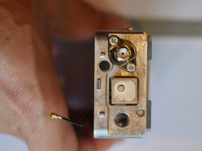
Teardown PCB Pictures
Port and Test Point Identification
Modules and Interconnects
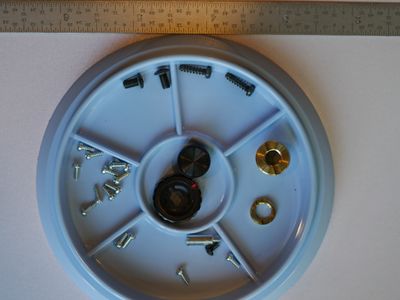
Mechanical Pictures
Reverse Engineering Efforts
High level goals
- Obtain a copy of the firmware for analysis/modification
- Understand how the radio works and what test ports are available internally
Obtaining firmware
- Determine routes of attack
- JTAG Port
- Serial Port
- Hardware attack - Remove Flash Memory and read directly (possibly encrypted/obfuscated)
- USB data capture - Packet capture firmware update (possibly encrypted/obfuscated)
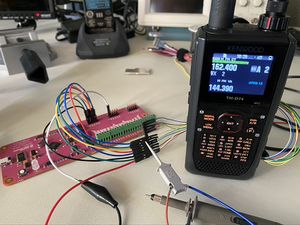
Initially the radio was opened and wires were soldered to some test points and an interesting PCB footprint that I suspected was JTAG as seen in the video below.
Serial Port
The serial port turned out to just be control data sent from the CPU board to the transceiver board, explained further below. Removing the flash memory is an option although it is a BGA package so not sure about soldering wires to it so it can be read out. Furthermore, the OMAP-L138 processor seems to have a few protection mechanisms. Encryption of the firmware is one of them so that route might be useless.
Hardware Attack
- Desolder flash memory chip
- Re-Ball BGA and clean in preparation for socket
- Insert into BGA socket and read contents using FlashCATUSB XPORT with BGA-64 (LAE064) socket
Other than the obvious challenge of desoldering and reballing a BGA, this worked great to get a complete image of the firmware! The firmware on the flash is not encrypted or obfuscated in any way so it's possible to make use of it immediately.
Cost breakdown to get complete firmware image using this method: $330 USD
- $145 - Replacement Processor board for TH-D74 (eBay)
- $40 - FlashcatUSB XPORT
- $145 - BGA-64 (LAE064) Socket
Having a copy of the firmware for modification and analysis... PRICELESS!
USB Data Capture
This method costs a lot less than the hardware attack, like $330 less! See the YouTube video below for a walk-through. The software tools used are listed below, I am sure other tools would work but this is what I used.
Have a better method? Create an account and update the wiki!
Hex Editor Neo - Allows bitwise operations and other cool features with a 14 day free trial!
USB Analyzer - By Eltima Software, it captures USB traffic and lets you easily export the binary data. It also comes with a 14 day free trial!
Firmware Parse Tool - Python program to strip header bytes from USB data captures
Understand how the radio works
There is a serial port labeled SCTX and SCRX (See Processor Board Bottom picture above), both of these lines appear to be transmit only from the top CPU board down to the bottom transceiver board. As the radio is tuned from one frequency to another the SCRX line has a lot of activity, when the transmitter is keyed up the SCTX line has activity. Below is a sample of what is seen on the SCRX line. Travis Goodspeed commented to me on Twitter that these commands seemed similar to the Rig Control commands sent from PC's to radio's to control them.
| SCRX |
|---|
| J0000 |
| K0000 |
| G0283 |
| `0 |
| G1283 |
| B06EE14 |
| B0A03CE |
| B0C0028 |
| B11E960 |
| B180000 |
| B140000 |
| B1C2812 |
| B200018 |
| B280A68 |
| G;7:3 |
| K1900 |
| a7:6 |
| B1C2C12 |
| B140000 |
| B1C2812 |
| B200018 |
| B280A68 |
| F41 |
| J01 |
| G;7:3 |
| `0 |
Datasheets
Kenwood TH-D74A Datasheet - IC-701 - DRAM
Kenwood TH-D74A Datasheet - IC-702 - omap-l138
Kenwood TH-D74A Datasheet - IC-705 - FLASH MEMORY
Using the OMAP-L138 Bootloader
IC-707 - Not exact match but same family - WM8940
